system and other user data files.
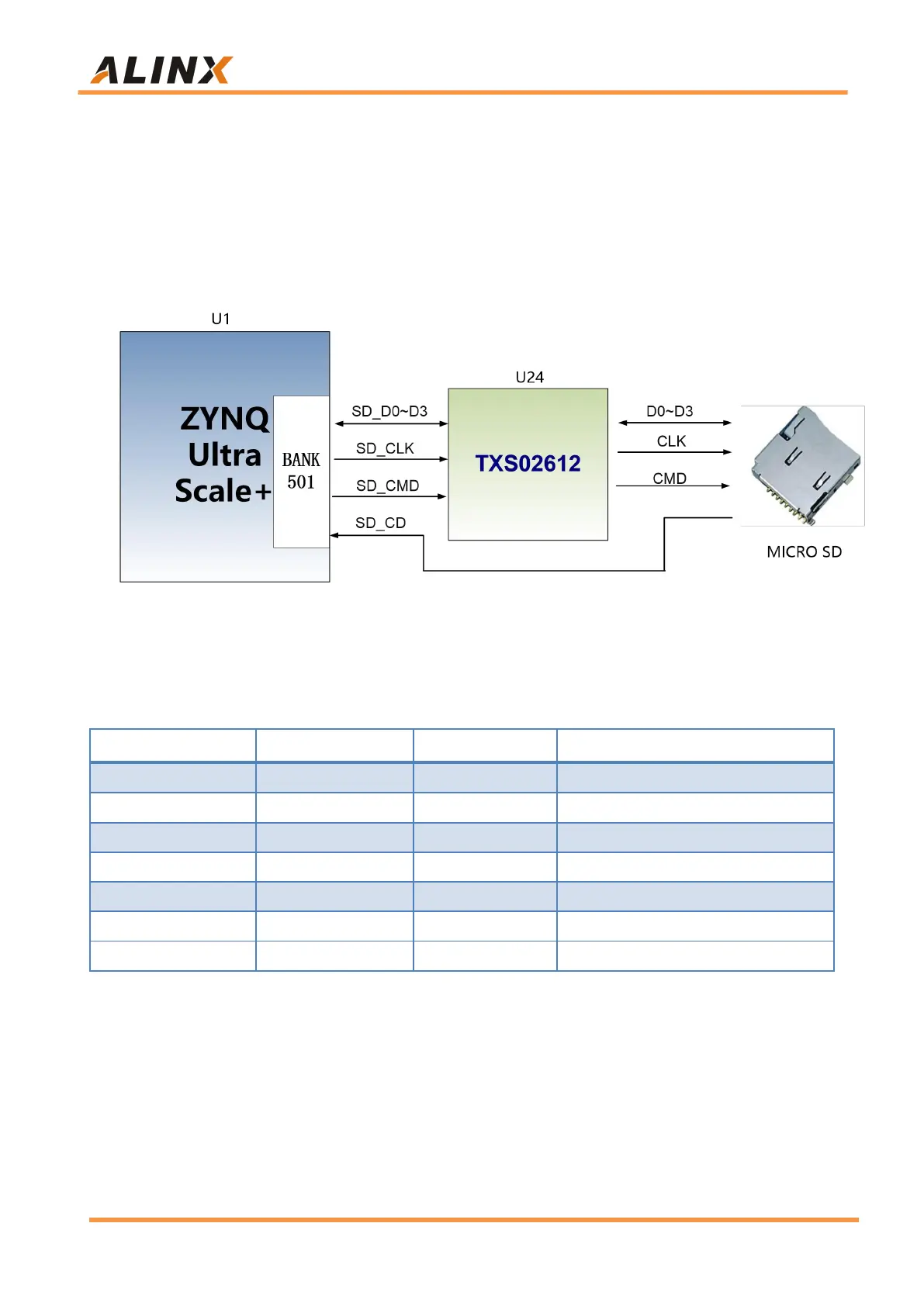
The SDIO signal is connected to the IO signal of the PS BANK501 of
ZU2CG. Since the VCCMIO of the BANK is set to 1.8V, but the data level of the
SD card is 3.3V, connected through the TXS02612 level shifter. The schematic
of the Zynq7000 PS and SD card connector is shown in Figure 3-10-1:
Figure 3-7-1: SD Card Connection Diagram
SD card slot pin assignment:
Part 3.8: Expansion Header
The AXU2CGB-E board is reserved with two 0.1-inch standard pitch 40-pin
expansion ports J45 and J46, which are used to connect the ALINX modules or
the external circuit designed by the user. The expansion port has 40 signals, of