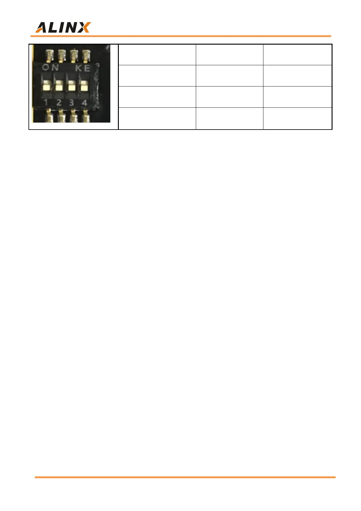
Table 3-17-1
Part 3.18: Power Supply
The power input voltage of the AXU2CGB-E development board is DC12V.
In the carrier board, the DC12V is converted into +5V, +3.3V, and +1.8V
through one-way DC/DC power chip TPS54620 and two-way DC/DC power
chip MP1482. In addition, the Carrier board generates +1.2V through LDO to
supply power to the core board BANK65, and the power supply of BANK66 is
+1.8V. The schematic diagram of the power supply design on the board is
shown in Figure 3-18-1: