below:
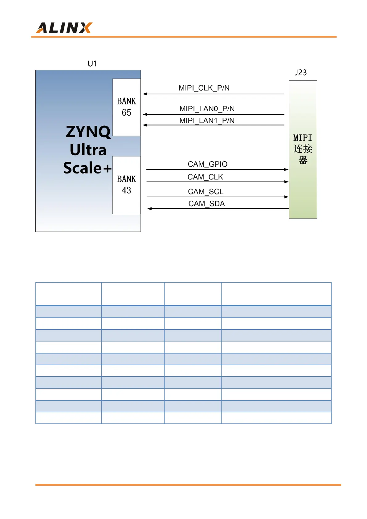
Figure 3-11-1: MIPI camera interface design schematic
MIPI interface pin assignment
MIPI Input Clock Positive
MIPI Input Clock Negative
MIPI Input Date LANE0 Positive
MIPI Input Date LANE0 Negative
MIPI Input Date LANE1 Positive
MIPI Input Date LANE1 Negative
Part 3.12: JTAG Debug Port
The JTAG interface is reserved on the AXU2CGB-E expansion board for