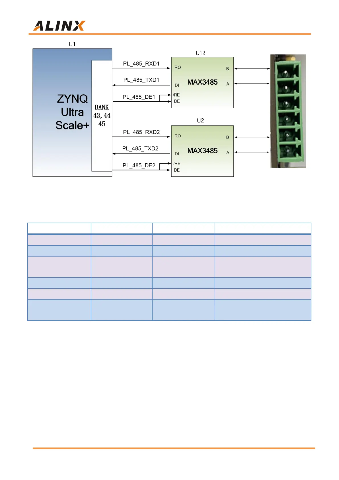
Figure 3-10-1: 485 Communication on the PL Side
The 485 communication pins are assigned as follows:
The 1
st
Channel 485 Transceiver
The 1
st
Channel 485 Receiver
The 1
st
Channel 485 Transmit
Enable
The 2
nd
Channel 485 Transceiver
The 2
nd
Channel 485 Receiver
The 2
nd
Channel 485 Transmit
Enable
Part 3.11: MIPI camera interface
The AXU2CGB-E carrier board includes a MIPI camera interface, which
can be used to connect with the ALINX Brand MIPI OV5640 camera module
AN5641. MIPI interface 15PIN FPC connector, 2 LANE data and 1 pair of clock,
connected to the differential IO pin of BANK65, the level standard is 1.2V; other
control signals are connected to the IO of BANK43, level standard It is 3.3V.
The circuit schematic of the MIPI interface part is shown in Figure 3-11-1