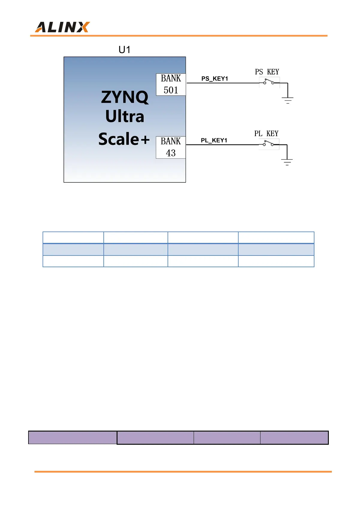
Figure 3-16-1: Rest keys connection diagram
ZYNQ pin assignment of keys
Part 3.17: DIP Switch Configuration
There is a 4-digit DIP switch SW1 on the FPGA development board to
configure the startup mode of the ZYNQ system. The AXU2CGB-E system
development platform supports 4 startup modes. The 4 startup modes are
JTAG debug mode, QSPI FLASH, EMMC and SD2.0 card startup mode. After
ZU2CG chip is powered on, it will detect the level of (PS_MODE0~3) to
determine the startup mode. The user can select different startup modes
through the DIP switch SW1 on the expansion board. The SW1 startup mode
configuration is shown in the following table 3-17-1.