EasyManua.ls Logo

Alinx AXU2CGB-E - Part 3.10: 485 Communication Interface

Alinx AXU2CGB-E
57 pages
Print Icon
To Next Page IconTo Next Page
To Previous Page IconTo Previous Page
Loading...
AXU2CGB-E User Manual
47
/
57
www.alinx.com
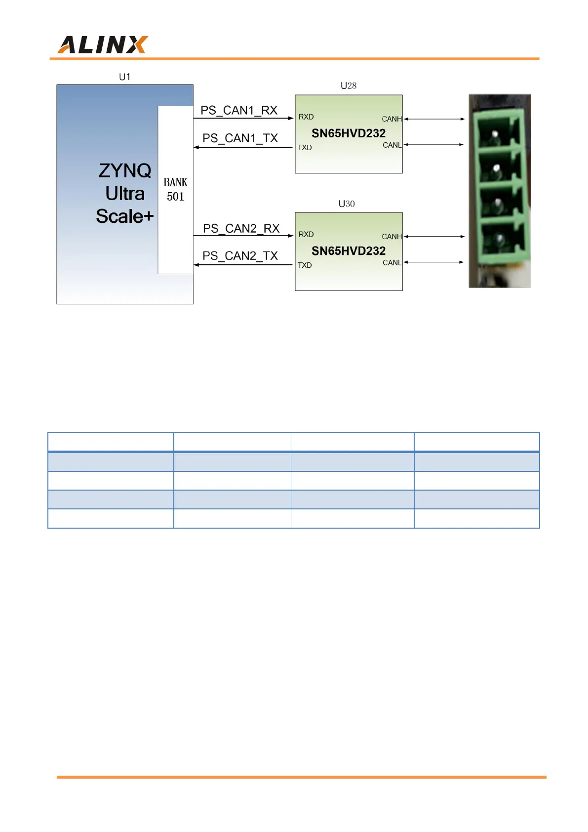
Figure 3-9-1: Connection diagram of CAN transceiver chip on PS side
The CAN communication pin assignments are as follows:
Signal Name
ZYNQ Pin Name
ZYNQ Pin Number
Description
PS_CAN1_TX
PS_MIO32
J16
CAN1 Receiver
PS_CAN1_RX
PS_MIO33
L16
CAN1 Transmitter
PS_CAN2_TX
PS_MIO39
H19
CAN2 Receiver
PS_CAN2_RX
PS_MIO38
H18
CAN2 Transmitter
Part 3.10: 485 communication interface
There are two 485 communication interfaces on the AXU2CGB-E carrier
board. The 485 communication port 1 is connected to the IO interface of
BANK43~45 on the PL system. The 485 transceiver chip selects the MAX3485
chip from MAXIM for the user's 485 communication service.
Figure 3-10-1 is the connection diagram of the 485 transceiver chip on the
PL side

Related product manuals