Part 1: FPGA Development Board Introduction
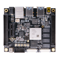
The entire structure of the AXU2CGB-E FPGA development board is
inherited from our consistent core board + carrier board model. A high-speed
inter-board connector is used between the core board and the carrier board.
The core board is mainly composed of the smallest system of XCZU2CG
+ 4 DDR4 + eMMC + QSPI FLASH, ACU2CG uses Xilinx's Zynq UltraScale+
MPSoCs CG chip, the model number is XCZU2CG-1SFVC784E. XCZU2CG
chip can be divided into processor system part Processor System (PS) and
programmable logic part Programmable Logic (PL). On the PS side of the
ZU2CG chip, there are 4 DDR4, each with a capacity of up to 512MB. The 8GB
eMMC FLASH memory chip and a 256Mb QSPI FLASH which are on the PS
side, used to statically store the operating system, file system and user data of
MPSoCs.
The AXU2CGB-E carrier board expands its rich peripheral interface,
including 1 SATA M.2 interface, 1 DP interface, 4 USB 3.0 Interface, 2 Gigabit
Ethernet interfaces, 1 SD card slot,2-Channel 40-pin expansion header,
2-Channel CAN bus interfaces, 2-Channel RS485 bus interfaces, 1 MIPI
Camera Interface and some keys and LEDs.
The following figure shows the structure of the entire development system: