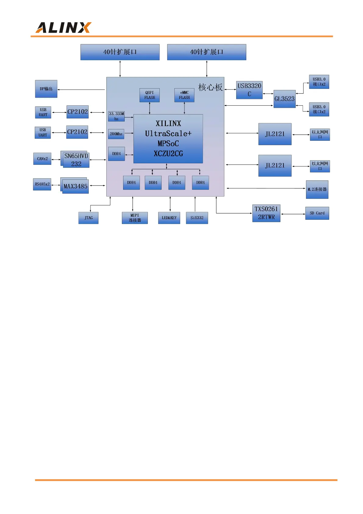
Figure 1-1-1: The Schematic Diagram of the AXU2CGB-E
Through this diagram, you can see the interfaces and functions that the
AXU2CGB-E FPGA Development Board contains:
ACU2CG core board
It consists of ACU2CG +4GB DDR4(PS)+8GB eMMC FLASH + 256Mb
QSPI FLASH, and there are 2 crystal oscillators to provide the clock, a
single-ended 33.3333MHz crystal oscillator for the PS system, and a
differential 200MHz crystal oscillator for the PL logic DDR reference
clock.
M.2 Interface1 PCIEx1 standard M.2 interface, used to connect M.2
SSD solid state drives, with a communication speed of up to 6Gbps.
DP Output Interface
1 standard Display Port output display interface, used for video image
display. Supports up to 4K@30Hz or 1080P@60Hz output
USB 3.0 Interface