Table 3-5-1: PHY chip default configuration value
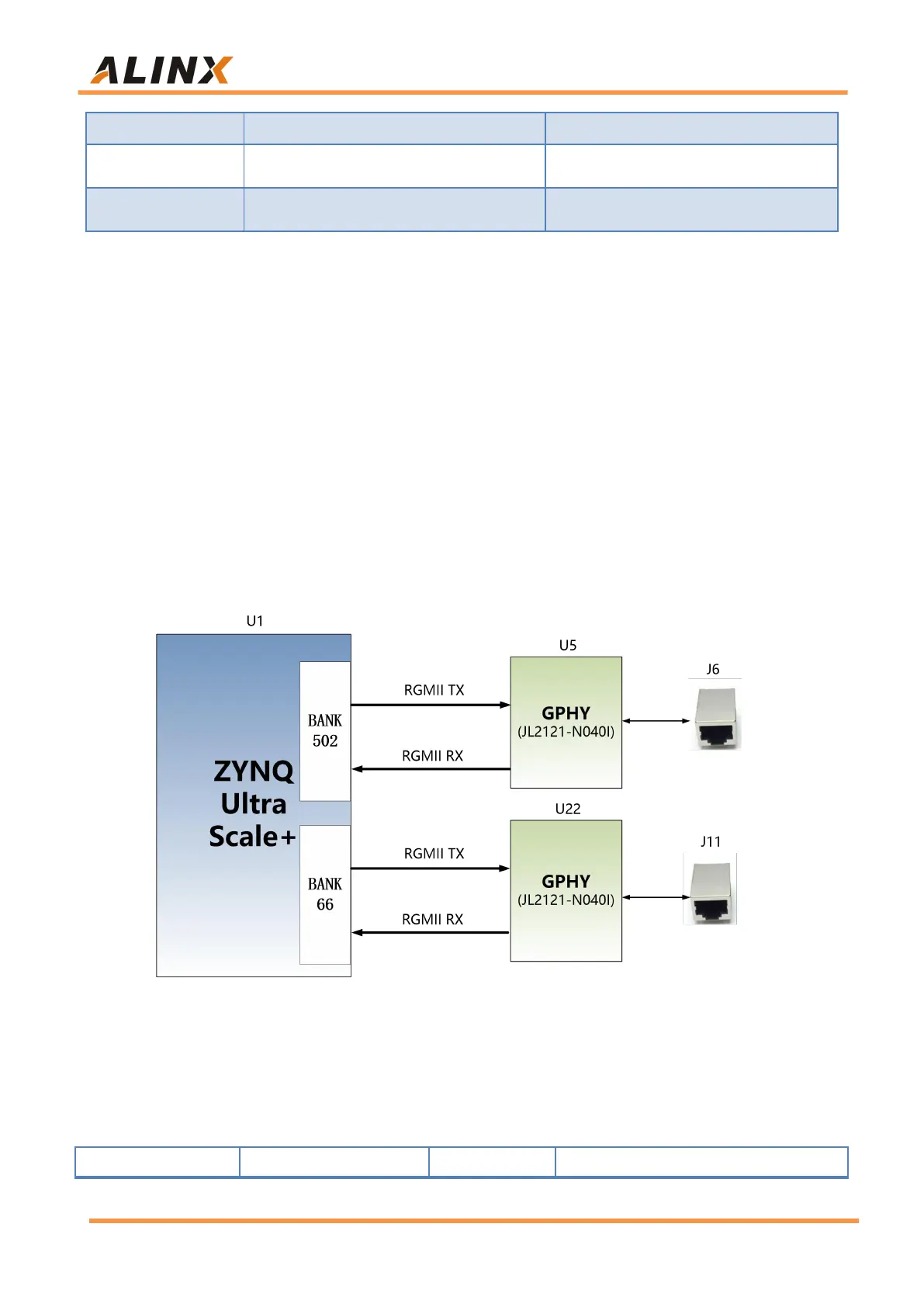
When the network is connected to Gigabit Ethernet, the data transmission
of ZYNQ and PHY chip JL2121-N040I is communicated through the RGMII bus,
the transmission clock is 125Mhz, and the data is sampled on the rising edge
and falling samples of the clock.
When the network is connected to 100M Ethernet, the data transmission of
ZYNQ and PHY chip JL2121-N040I is communicated through RMII bus, and
the transmission clock is 25Mhz. Data is sampled on the rising edge and falling
samples of the clock.
Figure 3-5-1: ZYNQ PS system and GPHY connection diagram
The Gigabit Ethernet pin assignments are as follows: