B–3Scan List Example
Publication
1756–6.5.15 – July 1998
Photoelectric Sensor Input Mapping Scheme Example
1756–DNB Communication Module Discrete Input Image Table
Photoelectric Sensor Input Bytes
photoelectric sensor node address 1 photoelectric sensor node address 2
photoelectric sensor node address 3 photoelectric sensor node address 4
1D1S
2D2S
3D3S
4D4S
1 byte
1 byte
1 byte
1 byte
1
The status and data bits
from each photoelectric
sensor are mapped into
the communication module’
s
input image table.
The input image table
is then transferred to the host
application.
1
2
0000 0000 0000 0000
0000 0000 0000 0000
0000 0000 0000 0000
0000 0000 0000 0000
0000 0000 0000 0000
Word 0
Word 1
Word 2
Word 3
Word 4
Input Image Table
1D2D3D 1S2S3S
word 0
2
word 1
4D
4S
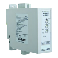
Allen-Bradley Drives
 Loading...