EasyManua.ls Logo

Altera DE2-115 - Serial Port

Altera DE2-115
116 pages
Print Icon
To Next Page IconTo Next Page
To Previous Page IconTo Previous Page
Loading...
54
Figure 4-23 Connections between FPGA and Audio CODEC
Table 4-17 Audio CODEC Pin Assignments
Signal Name
FPGA Pin No.
Description
I/O Standard
AUD_ADCLRCK
PIN_C2
Audio CODEC ADC LR Clock
3.3V
AUD_ADCDAT
PIN_D2
Audio CODEC ADC Data
3.3V
AUD_DACLRCK
PIN_E3
Audio CODEC DAC LR Clock
3.3V
AUD_DACDAT
PIN_D1
Audio CODEC DAC Data
3.3V
AUD_XCK
PIN_E1
Audio CODEC Chip Clock
3.3V
AUD_BCLK
PIN_F2
Audio CODEC Bit-Stream Clock
3.3V
I2C_SCLK
PIN_B7
I2C Clock
3.3V
I2C_SDAT
PIN_A8
I2C Data
3.3V
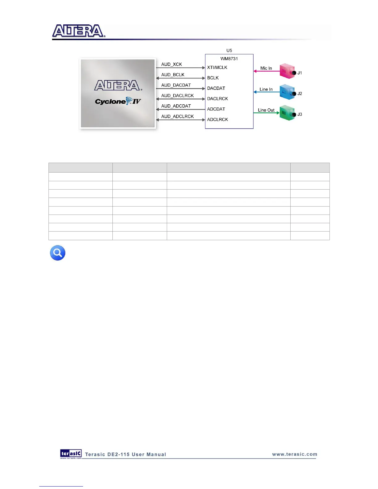
Note: If the HSMC loopback adapter is mounted, the I2C_SCL will be directly routed back
to I2C_SDA. Because audio chip, TV decoder chip and HSMC share one I2C bus, therefore
audio and video chip wont function correctly.
4
4
.
.
1
1
2
2
R
R
S
S
-
-
2
2
3
3
2
2
S
S
e
e
r
r
i
i
a
a
l
l
P
P
o
o
r
r
t
t
The DE2-115 board uses the ZT3232 transceiver chip and a 9-pin DB9 connector for RS-232
communications. For detailed information on how to use the transceiver, please refer to the
datasheet, which is available on the manufacturers website, or in the DE2_115_datasheets\RS-232
folder on the DE2-115 System CD. Figure 4-24 shows the related schematics, and Table 4-18 lists
the Cyclone IV E FPGA pin assignments.

Table of Contents

Related product manuals