4
4
.
.
5
5
C
C
l
l
o
o
c
c
k
k
C
C
i
i
r
r
c
c
u
u
i
i
t
t
r
r
y
y
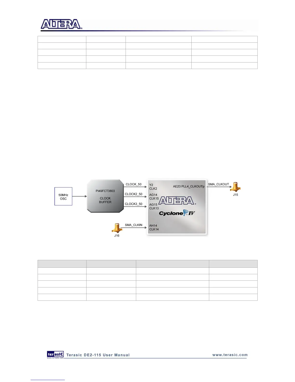
The DE2-115 board includes one oscillator that produces 50 MHz clock signal. A clock buffer is
used to distribute 50 MHz clock signal with low jitter to FPGA. The distributing clock signals are
connected to the FPGA that are used for clocking the user logic. The board also includes two SMA
connectors which can be used to connect an external clock source to the board or to drive a clock
signal out through the SMA connector. In addition, all these clock inputs are connected to the phase
locked loops (PLL) clock input pins of the FPGA to allow users to use these clocks as a source
clock for the PLL circuit.
The clock distribution on the DE2-115 board is shown in Figure 4-11. The associated pin
assignments for clock inputs to FPGA I/O pins are listed in Table 4-5.
Figure 4-11 Block diagram of the clock distribution
Table 4-5 Pin Assignments for Clock Inputs