4
4
.
.
1
1
7
7
U
U
s
s
i
i
n
n
g
g
t
t
h
h
e
e
U
U
S
S
B
B
I
I
n
n
t
t
e
e
r
r
f
f
a
a
c
c
e
e
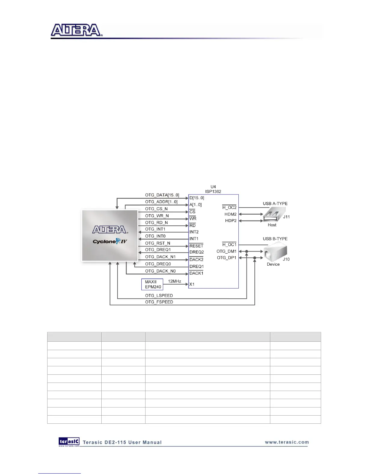
The DE2-115 board provides both USB host and device interfaces using the Philips ISP1362
single-chip USB controller. The host and device controllers are compliant with the Universal Serial
Bus Specification Rev. 2.0, supporting data transfer at full-speed (12 Mbit/s) and low-speed (1.5
Mbit/s). Figure 4-31 shows the schematic diagram of the USB circuitry; the pin assignments for the
associated interface are listed in Table 4-25.
Detailed information for using the ISP1362 device is available in its datasheet and programming
guide; both documents can be found on the manufacturer‟s website, or in the
DE2_115_datasheets\USB folder on the DE2-115 System CD. The most challenging part of a USB
application is in the design of the software driver needed. Two complete examples of USB drivers,
for both host and device applications, can be found in Sections 6.4 and 6.5. These demonstrations
provide examples of software drivers for the Nios II processor.
Figure 4-31 Connections between FPGA and USB (ISP1362)
Table 4-25 USB (ISP1362) Pin Assignments