4
4
.
.
1
1
9
9
U
U
s
s
i
i
n
n
g
g
S
S
R
R
A
A
M
M
/
/
S
S
D
D
R
R
A
A
M
M
/
/
F
F
L
L
A
A
S
S
H
H
/
/
E
E
E
E
P
P
R
R
O
O
M
M
/
/
S
S
D
D
C
C
a
a
r
r
d
d
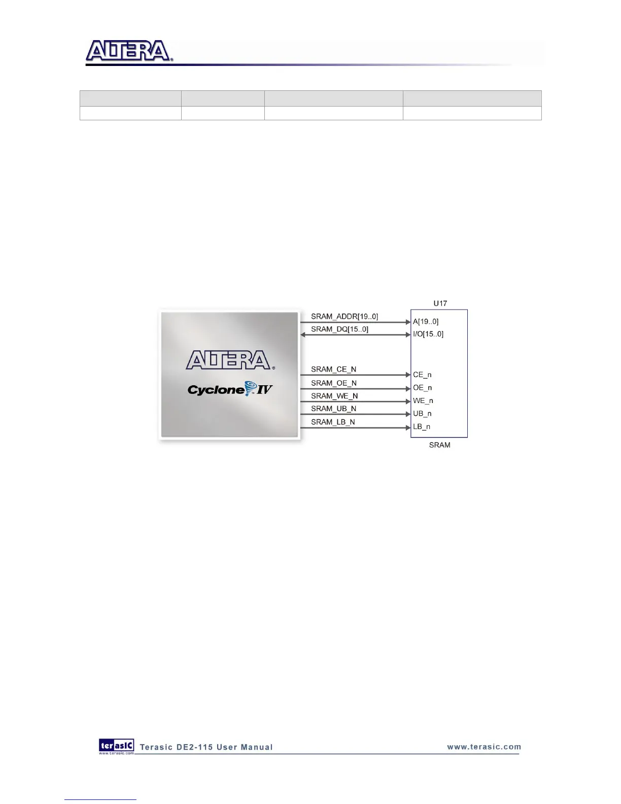
SRAM
The DE2-115 board has 2MB SRAM memory with 16-bit data width. Being featured with a
maximum performance frequency of about 125MHz under the condition of standard 3.3V single
power supply makes it suitable of dealing with high-speed media processing applications that need
ultra data throughput. The related schematic is shown in Figure 4-33.
Figure 4-33 Connections between FPGA and SRAM
SDRAM
The board features 128MB of SDRAM, implemented using two 64MB SDRAM devices. Each
device consists of separate 16-bit data lines connected to the FPGA, and shared control and address
lines. These chips use the 3.3V LVCMOS signaling standard. Connections between FPGA and
SDRAM are shown in Figure 4-34.