SECTION 6 PERFORMANCE TESTS
6-53
Input attenuator (RF ATT) switching uncertainty
At this point, measure the switching error when the amount of attenuation in the RF input section is switched.
When the input attenuator is switched, IF-section step-amplifier gain is switched. To keep this step-amplifier
gain constant, the reference level is switched according to the amount of input attenuator attenuation.
(1) Specifications
• Input attenuator switching error: ± 0.3 dB (at 0 to 50 dB, frequency 100 MHz and input ATT 10 dB)
(2) Test instruments
• Signal generator: MG3633A
• Attenuator: MN510C
• Power meter: ML2437A
• Power sensor: MA2422A
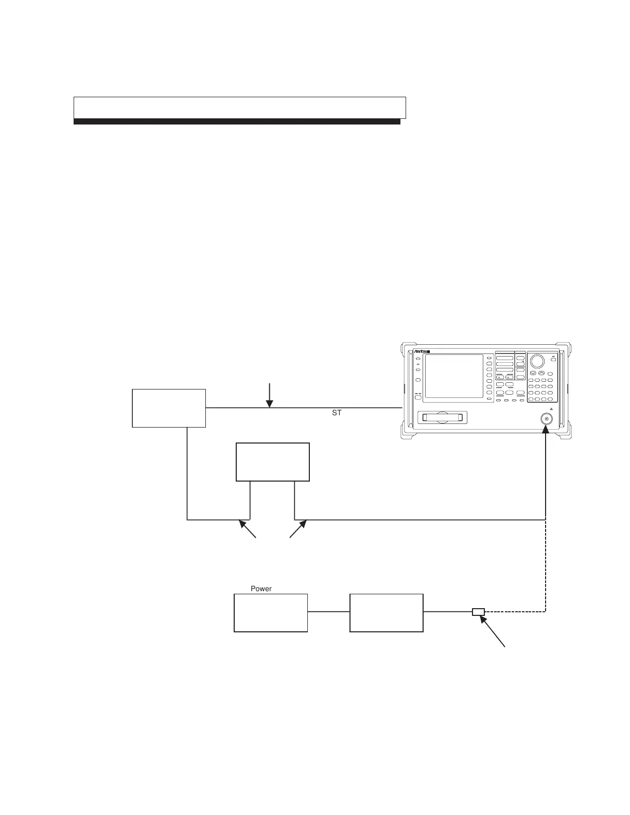
(3) Setup
RF OUTPUT
OUTPUT
INPUT
RF Input
Signal generator
REF
IN
MG3633A
Coaxial cable
(N connector)
Coaxial connector
(BNC connector)
Attenuator
MN510C
Power meter
ML2437A
Power Sensor
MA2422A
Coaxial adaptor
(N-J·N--J)
10MHz STD
Buff Out
(Note)
Input Attenuator Switching Error Test
(Note) In case of MS2665C, if there is no buffer output for the reference oscillator (Option 01)
on the rear panel, input a reference signal from an external 10 MHz frequency standard
to the main body and signal generator.
Stby
Shift
On
Preset
Menu On/Off
More
RBW VBW Sweep Time Atten
Local
Remote
F1
F2
F3
F4
F5
F6
Display
Coupled Function
MS2665C
Spectrum Analyzer
9kHz–21.2GHz
PTA Define
Memory Card
Enter
Hold
µv
µsec
EntryMarkerFreq/Ampl
7
Copy Cont
Copy
8 9 GHz
CE
4 5 6 MHz
BS
+/–
3
mV
msec
dBm
dB
V
sec
Cal
Interface Mem Card
Sound System Title
1 2 kHz
0 • Hz
A/B.A/BG A/Time
Save
Recall
Amplitude
Span
Frequency
Measure
A.B Time Trig/Gate
Peak
Continuous
CF RLV Single
Marker
Peak
Search
Multi Mkr
Marker
User
RF Input 50Ω
+30dBm
0V DC Max