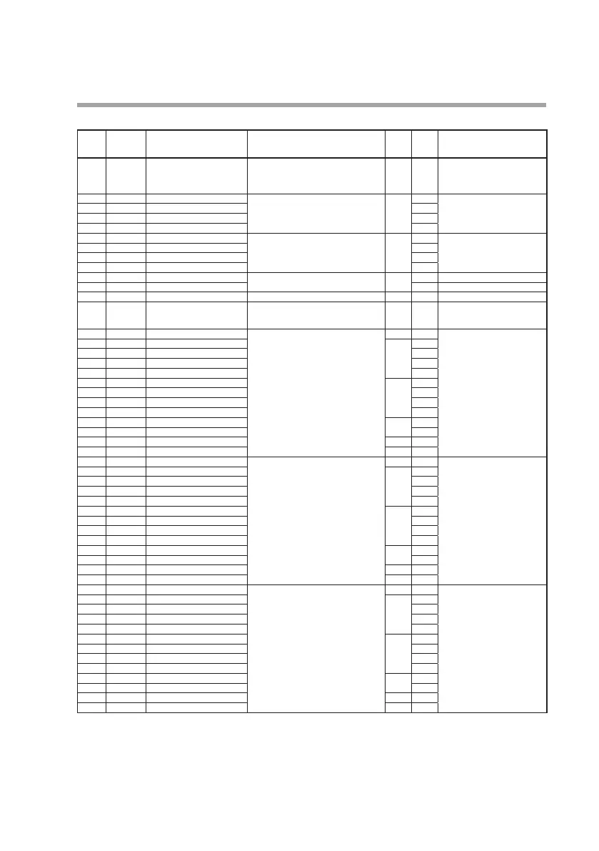
2-29
Chapter 2. PARA BANK SETTINGS
Logical operation bank (bf)
Display
Logical opera-
tion number
(auxiliary display)
Item Settings and descriptions Initial
value
User
setting
Remarks
bF-0
1 0
1.
Operation type 1: Operation 1 (A and B) or (C and D)
2: Operation 2 (A or B) and (C or D)
3: Operation 3 (A or B or C or D)
4: Operation 4 (A and B and C and D)
1
bF-02 0
1.
Input assignment A 1024 to 2047 1024 For details, refer to: Standard bit
codes (P.4-1).
bF-03 0
1.
Input assignment B
bF-04 0
1.
Input assignment C
bF-05 0
1.
Input assignment D
bF-06 0
1.
Input bit polarity A 0: Direct 1: Reverse 0
bF-07 0
1.
Input bit polarity B
bF-08 0
1.
Input bit polarity C
bF-09 0
1.
Input bit polarity D
bF-
10 0
1.
ON delay time 0.0 to 3200.0 s 0.0
bF-
1
1 0
1.
OFF delay time
bF-
12 0
1.
Polarity 0: Direct 1: Reverse 0
bF-
13 0
1.
Latch 0: None 1: Latch at ON
2: Latch at OFF (except for initialization
at OFF)
0
bF-0
1 02.
Operation type Same as logical operation 1
1
Same as logical operation 1
bF-02 02.
Input assignment A 1024
bF-03 02.
Input assignment B
bF-04 02.
Input assignment C
bF-05 02.
Input assignment D
bF-06 02.
Input bit polarity A 0
bF-07 02.
Input bit polarity B
bF-08 02.
Input bit polarity C
bF-09 02.
Input bit polarity D
bF-
10 02.
ON delay time 0.0
bF-
1
1 02.
OFF delay time
bF-
12 02.
Polarity 0
bF-
13 02.
Latch 0
bF-0
1 03.
Operation type Same as logical operation 1
1
Same as logical operation 1
bF-02 03.
Input assignment A 1024
bF-03 03.
Input assignment B
bF-04 03.
Input assignment C
bF-05 03.
Input assignment D
bF-06 03.
Input bit polarity A 0
bF-07 03.
Input bit polarity B
bF-08 03.
Input bit polarity C
bF-09 03.
Input bit polarity D
bF-
10 03.
ON delay time 0.0
bF-
1
1 03.
OFF delay time
bF-
12 03.
Polarity 0
bF-
13 03.
Latch 0
bF-0
1 04.
Operation type Same as logical operation 1
1
Same as logical operation 1
bF-02 04.
Input assignment A 1024
bF-03 04.
Input assignment B
bF-04 04.
Input assignment C
bF-05 04.
Input assignment D
bF-06 04.
Input bit polarity A 0
bF-07 04.
Input bit polarity B
bF-08 04.
Input bit polarity C
bF-09 04.
Input bit polarity D
bF-
10 04.
ON delay time 0.0
bF-
1
1 04.
OFF delay time
bF-
12 04.
Polarity 0
bF-
13 04.
Latch 0