86
74HC4067M96 16-Channel Demultiplexer
Integrated Circuit Diagrams
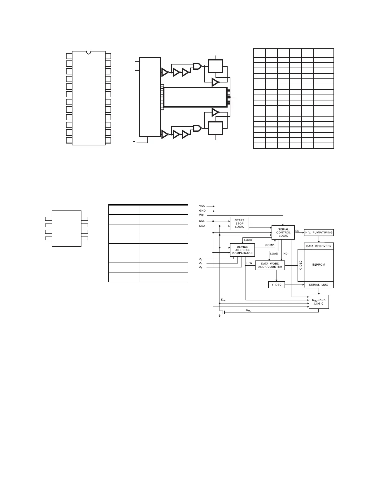
AT24C04N-10SU-2.7 EEPROM
TOP VIEW
1
2
3
4
5
6
7
8
9
10
11
12
COMMON
I
7
I
6
I
5
I
4
I
3
I
2
I
1
I
0
S
0
S
1
GND
16
17
18
19
20
21
22
23
24
15
14
13
V
CC
I
9
I
10
I
11
I
12
I
14
E
S
2
S
3
I
8
I
13
I
15
INPUT/OUTPUT
Functional Diagram
TRUTH TABLE
S0 S1 S2 S3 E
SELECTED
CHANNEL
XXXX1 None
00000 0
10000 1
01000 2
11000 3
00100 4
10100 5
01100 6
11100 7
00010 8
10010 9
01010 10
11010 11
00110 12
10110 13
01110 14
11110 15
H= High Level
L= Low Level
X= Don’t Care
PN
I
0
9
PN
I
15
16
14 - OUTPUT CIRCUITS
SAME AS ABOVE
(WITH ANALOG INPUTS)
I
1
TO I
14
BINARY
1 OF 16
DECODER
S
N
= 5 STAGES
E = 4 STAGES
10
11
14
13
S
3
S
2
S
1
S
0
E
15
1
COMMON
INPUT/
OUTPUT
Pin Configuration
Pin Name Function
A0 - A2 Address Inputs
SDA Serial Data
SCL Serial Clock Input
WP Write Protect
NC No Connect
GND Ground
VCC Power Supply
Pinout Diagram
8-lead SOIC
1
2
3
4
8
7
6
5
A0
A1
A2
GND
VCC
WP
SCL
SDA
Block Diagram
Pin Descriptions
SERIAL CLOCK (SCL): The SCL input is used to positive edge clock data into each
EEPROM device and negative edge clock data out of each device.
SERIAL DATA (SDA): The SDA pin is bidirectional for serial data transfer. This pin is
open-drain driven and may be wire-ORed with any number of other open-drain or open-
collector devices.
DEVICE/PAGE ADDRESSES (A2, A1, A0): The A2, A1 and A0 pins are device
address inputs.
The AT24C04 uses the A2 and A1 inputs for hard wire addressing and
a total of four 4Kdevices may be addressed on a single bus system. The A0 pin is a
no connect.
WRITE PROTECT (WP): The AT24C01A/02/04/08A/16A has a Write Protect pin that
provides hardware data protection. The Write Protect pin allows normal Read/Write
operations when connected to ground (GND). When the Write Protect pin is connected
to V
CC
, the write protection feature is enabled.