87
Integrated Circuit Diagrams
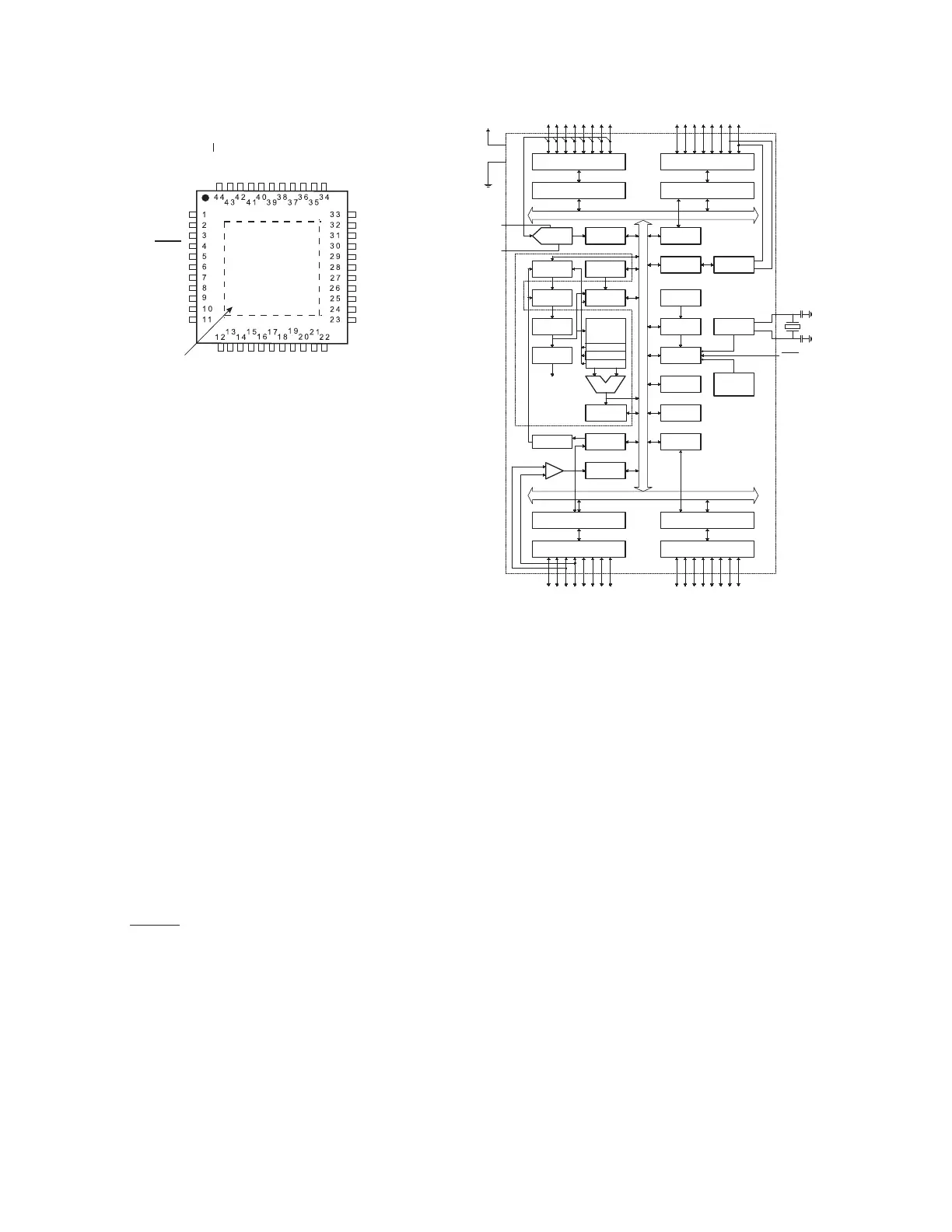
ATMEGA16L Microprocessor
PA4 (ADC4)
PA5 (ADC5)
PA6 (ADC6)
PA7 (ADC7)
AREF
GND
AVCC
PC7 (TOSC2)
PC6 (TOSC1)
PC5 (TDI)
PC4 (TDO)
(MOSI) PB5
(MISO) PB6
(SCK) PB7
RESET
VCC
GND
XTAL2
XTAL1
(RXD) PD0
(TXD) PD1
(INT0) PD2
(INT1) PD3
(OC1B) PD4
(OC1A) PD5
(ICP1) PD6
(OC2) PD7
VCC
GND
(SCL) PC0
(SDA) PC1
(TCK) PC2
(TMS) PC3
PB4 (SS)
PB3 (AIN1/OC0)
PB2 (AIN0/INT2)
PB1 (T1)
PB0 (XCK/T0)
GND
VCC
PA0 (ADC0)
PA1 (ADC1)
PA2 (ADC2)
PA3 (ADC3)
TQFP44 PACKAGE
NOTE:
Bottom pad should
be soldered to ground.
Block Diagram
INTERNAL
OSCILLATOR
OSCILLATOR
WATCHDOG
TIMER
MCU CTRL.
& TIMING
OSCILLATOR
TIMERS/
COUNTERS
INTERRUPT
UNIT
STACK
POINTER
EEPROM
SRAM
STATUS
REGISTER
USART
PROGRAM
COUNTER
PROGRAM
FLASH
INSTRUCTION
REGISTER
INSTRUCTION
DECODER
PROGRAMMING
LOGIC
SPI
ADC
INTERFACE
COMP.
INTERFACE
PORTA DRIVERS/BUFFERS
PORTA DIGITAL INTERFACE
GENERAL
PURPOSE
REGISTERS
X
Y
Z
ALU
+
-
PORTC DRIVERS/BUFFERS
PORTC DIGITAL INTERFACE
PORTB DIGITAL INTERFACE
PORTB DRIVERS/BUFFERS
PORTD DIGITAL INTERFACE
PORTD DRIVERS/BUFFERS
XTAL1
XTAL2
RESET
CONTROL
LINES
VCC
GND
MUX &
ADC
AREF
7CP - 0CP7AP - 0AP
PD0 - PD7PB0 - PB7
AVR CPU
TWI
AVC C
INTERNAL
CALIBRATED
OSCILLATOR
Pin Descriptions
VCC Digital supply voltage.
GND Ground.
Port A (PA7..PA0) Port A serves as the analog inputs to the A/D Converter.
Port A also serves as an 8-bit bi-directional I/O port, if the A/D Converter is not used.
Port B (PB7..PB0) Port B is an 8-bit bi-directional I/O port with internal pull-up resistors (selected for each
bit). The Port B output buffers have symmetrical drive characteristics with both high sink
and source capability.
Port C (PC7..PC0) Port C is an 8-bit bi-directional I/O port with internal pull-up resistors (selected for each
bit). The Port C output buffers have symmetrical drive characteristics with both high sink
and source capability.
Port D (PD7..PD0) Port D is an 8-bit bi-directional I/O port with internal pull-up resistors (selected for each
bit). The Port D output buffers have symmetrical drive characteristics with both high sink
and source capability.
RESET
Reset Input. A low level on this pin for longer than the minimum pulse length will gener-
ate a reset, even if the clock is not running.
XTAL1 Input to the inverting Oscillator amplifier and input to the internal clock operating circuit.
XTAL2 Output from the inverting Oscillator amplifier.
AVCC AVCC is the supply voltage pin for Port A and the A/D Converter. It should be externally
connected to VCC
, even if the ADC is not used.
AREF AREF is the analog reference pin for the A/D Converter.