88
Integrated Circuit Diagrams
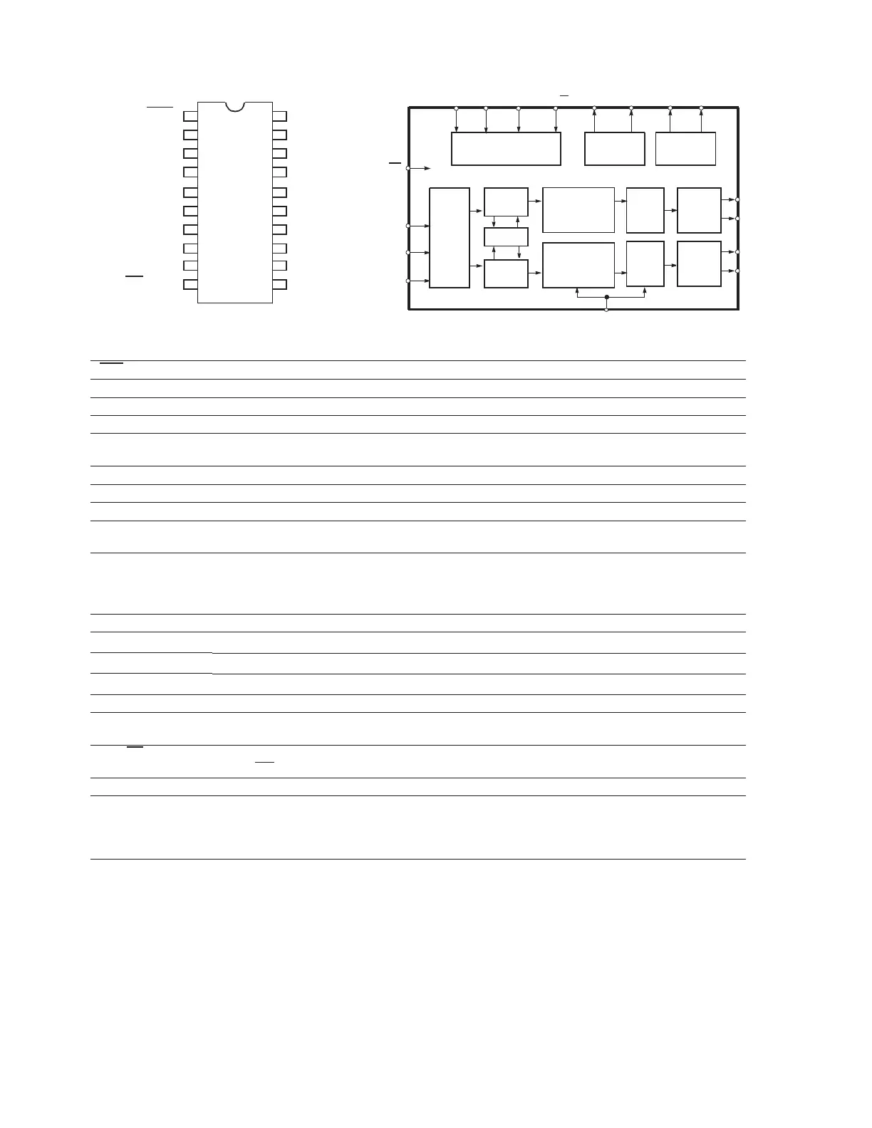
CS4392-KZ Digital to Analog Converter
LRCK
SDATA
(SDA/CDIN)
MCLK
AMUTEC
AOUTA-
AOUTB-
SERIAL
PORT
INTERPOLATION
INTERPOLATION
(CONTROL PORT)
∆Σ
DAC
DAC
EXTERNAL
ANALOG
FILTER
ANALOG
FILTER
∆Σ
MUTE CONTROL
FILTER
FILTER
RST
SCLK
VOLUME
CONTROL
VOLUME
CONTROL
MIXER
(SCL/CCLK) (AD0/CS)
AOUTA+
AOUTB+
CMOUT
REFERENCE
FILT+BMUTEC
M1
M3
M2
MODE SELECT
M0
RST 1 Reset (Input) - Powers down device and resets all internal registers to their default settings.
VL 2 Logic Power (Input) - Positive power for the digital input/output.
SDATA 3 Serial Audio Data (Input) - Input for two’s complement serial audio data.
SCLK 4 Serial Clock (Input/Output) - Serial clock for the serial audio interface.
LRCK 5 Left Right Clock (Input/Output) - Determines which channel, Left or Right, is currently active on the
serial audio data line.
MCLK 6 Master Clock (Input) - Clock source for the delta-sigma modulator and digital filters.
FILT+ 11 Positive Voltage Reference (Output) - Positive reference voltage for the internal sampling circuits.
CMOUT 12 Common Mode Voltage (Output) - Filter connection for internal quiescent voltage.
AMUTEC
BMUTEC
20
13
Mute Control (Output) - The Mute Control pin goes high during power-up initialization, reset, muting,
power-down or if the master clock to left/right clock frequency ratio is incorrect.
AOUTB-
AOUTB+
AOUTA+
AOUTA
14
15
18
19
Differential Analog Output (Outputs) - The full scale differential analog output level is specified in the
Analog Characteristics specification table.
AGND 16 Ground (Input)
VA
17 Analog Power (Input) - Positive power for the analog section.
Control Port Mode Definitions
M3
7 Mode Selection (Input) - This pins should be tied to GND level during control port mode.
SCL/CCLK 8 Serial Control Port Clock (Input) - Serial clock for the serial control port.
SDA/CDIN 9 Serial Control Data (Input/Output) - SDA is a data I/O line in I
2
C mode. CDIN is the input data line for
the control port interface in SPI mode.
AD0/CS
10 Address Bit 0 (I
2
C) / Control Port Chip Select (SPI) (Input/Output) - AD0 is a chip address pin in I
2
C
mode; CS
is the chip select signal for SPI format.
Stand-Alone Mode Definitions
M3
M2
M1
M0
7
8
9
10
Mode Selection (Input) - Determines the operational mode of the device.
RST AMUTEC
-ATUOALV
+ATUOAATADS
AVKLCS
DNGAKCRL
+BTUOAKLCM
-BTUOA3M
(CETUMB2M)KLCC/LCS
(TUOMC1M)NIDC/ADS
(AD0/CS
+TLIF0M)
1
2
3
4
20
19
18
17
5
6
7
8
16
15
14
13
9
10
12
11