90
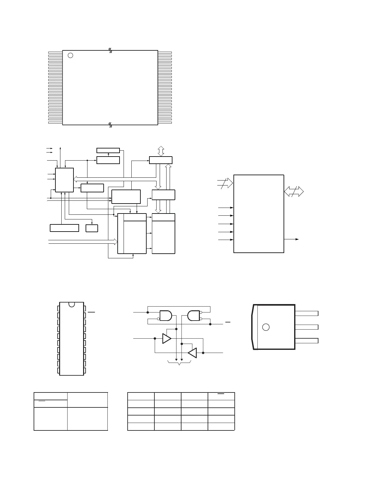
Integrated Circuit Diagrams
S29AL004D-90TF102 4M Flash
Block Diagram
Input/Output
Buffers
X-Decoder
Y-Decoder
Chip Enable
Output Enable
Logic
Erase Voltage
Generator
PGM Voltage
Generator
Timer
V
CC
Detector
State
Control
Command
Register
V
CC
V
SS
WE#
BYTE#
CE#
OE#
STB
STB
DQ0– DQ15 (A-1)
Sector Switches
RY/BY#
RESET#
Data
Latch
Y-Gating
Cell Matrix
Address Latch
A0–A17
Connection Diagrams
A1
A15
NC
A14
A13
A12
A11
A10
A9
A8
NC
NC
WE#
R
ESET#
NC
NC
RY/BY#
A17
A7
A6
A5
A4
A3
A2
1
16
2
3
4
5
6
7
8
17
18
19
20
21
22
23
24
9
10
11
12
13
14
15
A16
DQ2
BYTE#
V
SS
DQ15/A-1
DQ7
DQ14
DQ6
DQ13
DQ9
DQ1
DQ8
DQ0
OE#
V
SS
CE#
A0
DQ5
DQ12
DQ4
V
CC
DQ11
DQ3
DQ10
48
33
47
46
45
44
43
42
41
40
39
38
37
36
35
34
25
32
31
30
29
28
27
26
Standard TSOP
Logic Symbol
18
16 or 8
DQ0–DQ15
(A-1)
A0–A17
CE#
OE#
WE#
RESET#
BYTE# RY/BY#
Pin Configuration
A0–A17 = 18 addresses
DQ0–DQ14 = 15 data inputs/outputs
DQ15/A-1 = DQ15 (data input/output, word
mode),
A-1 (LSB address input, byte
mode)
BYTE# = Selects 8-bit or 16-bit mode
CE# = Chip enable
OE# = Output enable
WE# = Write enable
RESET# = Hardware reset pin, active low
RY/BY# = Ready/Busy# output
V
CC
= 3.0 volt-only single power supply
(see Product Selector Guide for speed
options and voltage supply tolerances)
V
SS
= Device ground
NC = Pin not connected internally
terminal assignments
1234
A A1
DIR V
CC
OE
B A3 B2 A2 B1
C A5 A4 B4 B3
D A7 B6 A6 B5
E GND A8 B8 B7
function table
INPUTS
OE DIR
OPERATION
L L B data to A bus
L H A data to B bus
H X Isolation
logic diagram (positive logic)
DIR
OE
A1
B1
To Seven Other Channels
1
2
19
18
1
2
3
4
5
6
7
8
9
10
20
19
18
17
16
15
14
13
12
11
DIR
A1
A2
A3
A4
A5
A6
A7
A8
GND
V
CC
OE
B1
B2
B3
B4
B5
B6
B7
B8
(TOP VIEW)
SN74LV245ADWR Octal B Transceiver
LT1587CM
V
IN
V
OUT
ADJ
FRONT VIEW
3
2
1
LT1587CM Regulator