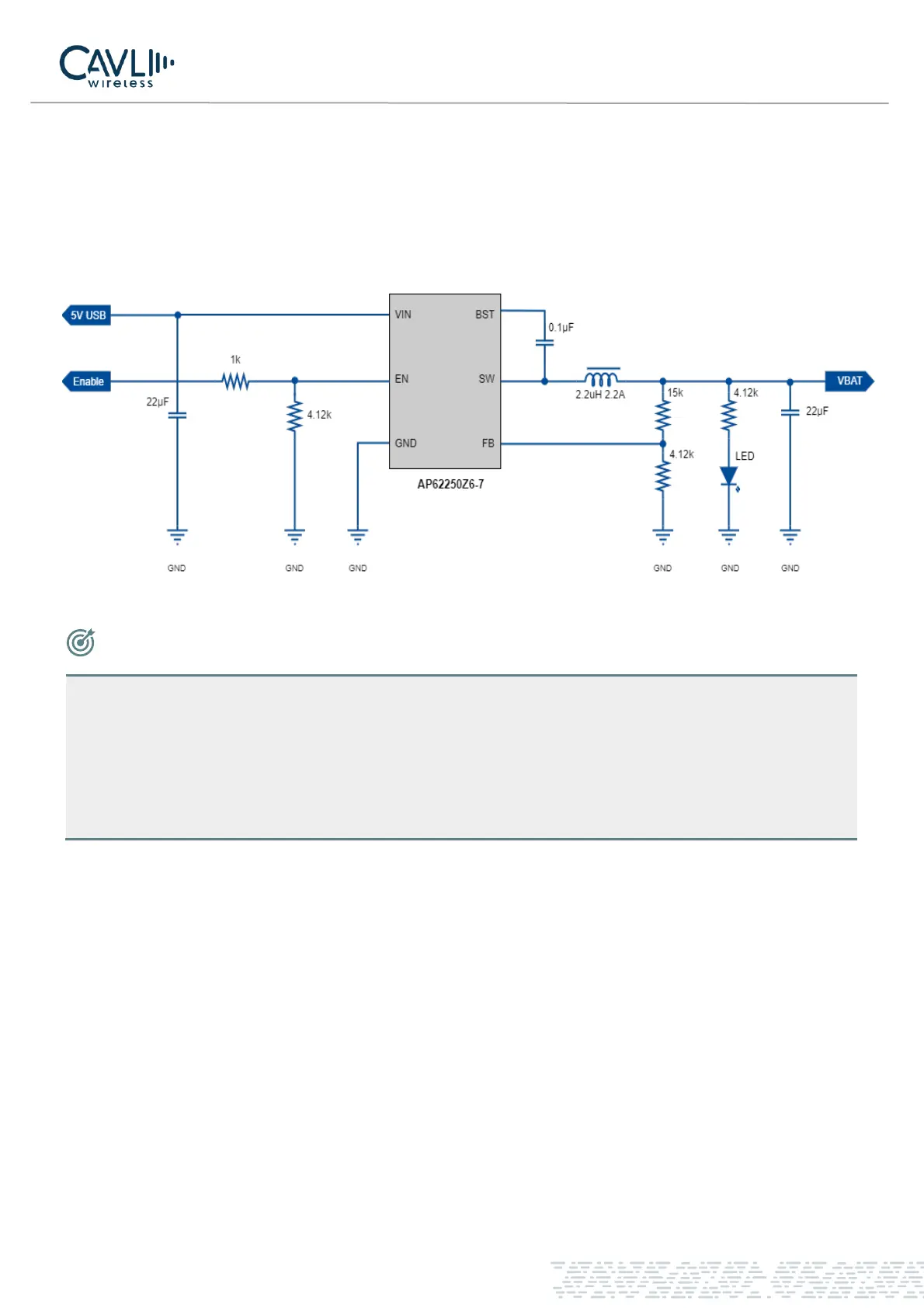
3.3.2 Power Reference Circuit
A linear LDO power supply to design the VBAT power supply. For better understanding, refer the circuit given
below.
Figure 4 LDO linear power reference circuit
NOTE
• In order to prevent the module from being damaged by surge and overvoltage, a 5.1V/500mW
Zener diode is suggested to be connected in parallel at the VBAT pin of the module.
• It is suggested that 3 ceramic capacitors (33pF, 10pF, 100nF) be added to the VBAT line and
placed near the VBAT pin.
3.3.3 VREF 1.8 Voltage Output
The C16QS module outputs 1.8V through VREF for internal digital circuitry. This voltage is the logic level
voltage of the module. After normal power-on, the 29
th
pin will output 1.8V and the current load will be 50mA.
The external master can read the voltage of VREF to determine if the module is powered on. VREF can also be
used as an external power supply, such as a level shifting chip, but maximum load should be within 50mA.