1PPS:
Synchronized at rising edge, and the pulse width is 500ms. This pin must be low at start-up for normal operation.
It has been pulled down internally with a 47KΩ resistor. If unused, keep this pin open.
GNSS interface
GNNSS_TXD and GNSS_RXD pins are used for fetching NMEA logs.
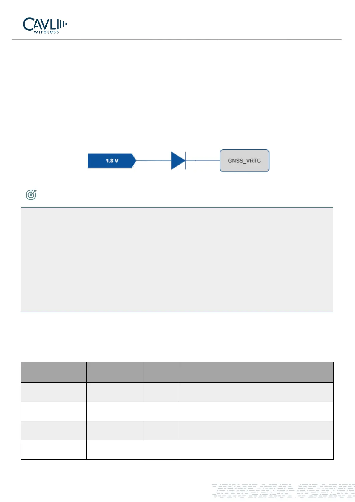
GNSS RTC Battery
This pin is the power input of the RTC battery. The module can store the data if the GNSS_VRTC pin is supplied
with 1.8 voltage.
Figure 25 GNSS VRTC Input
NOTE
• The recommended voltage rating of GNSS_VDD is 3.3 V.
• To enable GNSS, the voltage level of GNSS_EN should not go below 1.2V and should not exceed 1.8V.
• UART2 and GNSS UART are internally connected so while using GNSS ensure that UART 2 is kept as
floating and vice versa.
• When GNSS is operating in independent mode, only GNSS_VDD needs to be supplied; VBAT is not
required.
As VBATT_RF powers the entire RF of LTE and GNSS. GNSS_VDD can power entire GNSS section
• Please refer the C16QS GNSS Application note for further information.
3.17 SPI Interface
Table 3-27 SPI interface pin definition
Master output slave input
Master input slave output