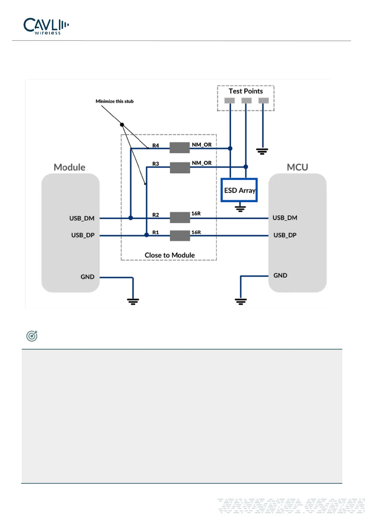
The module only acts as a USB slave device and supports USB Sleep and Wake-Up mechanisms. USB interface
application reference circuit is as follows:
Figure 7 USB connection design circuit diagram
NOTE
• Required a resistance of 16R for R1/R2.
• The USB interface supports high-speed (480Mbps) and full-speed (12Mbps) modes, so the trace
design needs to strictly follow the USB2.0 protocol requirements, pay attention to the protection
of the data line, differential trace, control impedance is 90Ω.
• In order to improve the antistatic performance of the USB interface, it is recommended to add an
ESD protection device on the data line. The equivalent capacitance of the protection device is less
than 2pF.
• The USB interface bus supply voltage is provided internally by the module and does not need to
be externally supplied. At the same time, since the USB interface of the module does not provide
USB bus power, the module can only be used as a slave device of the USB bus device.