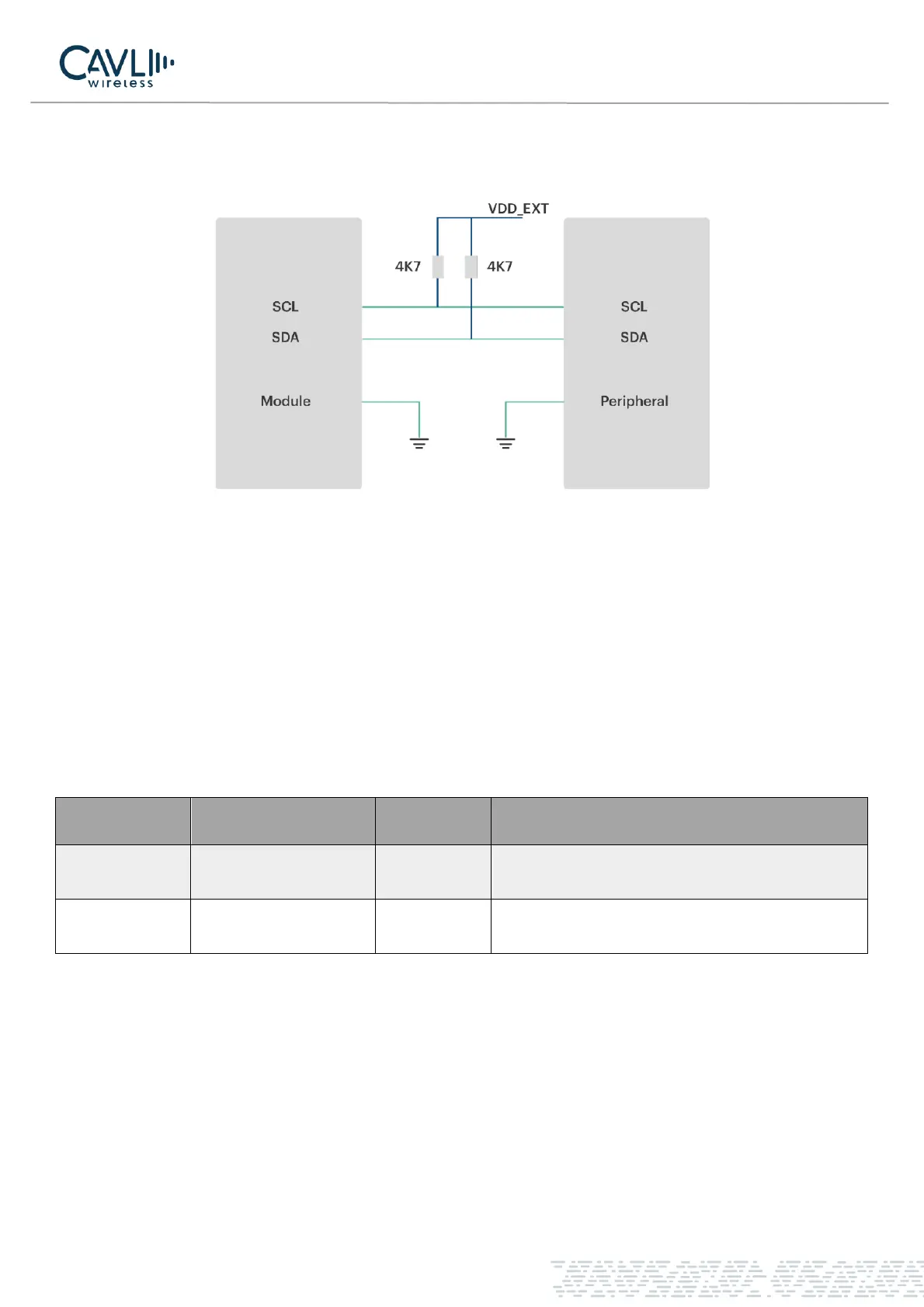
The I2C reference circuit is connected as follows:
Figure 14 I2C interface reference circuit diagram
3.12 SWD Interface
C16QS module provides a 2-pin serial wire debug (SWD) interface which is an alternative to JTAG.
Table 3-21 SWDIO Pin Definitions
3.13 ADC Interface
The C16QS provides two analog-to-digital converter interfaces to read the voltage value.
✓ The ADC interface input voltage cannot exceed VBAT
✓ It is recommended that the ADC pin be input with a voltage divider circuit