Parameter
structure
Keypad and
display
Parameter x.00
Parameter
description format
Advanced parameter
descriptions
Serial comms
protocol
Electronic
nameplate
Performance
Menu 6
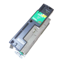
Digitax ST Advanced User Guide 97
Issue Number: 1 www.controltechniques.com
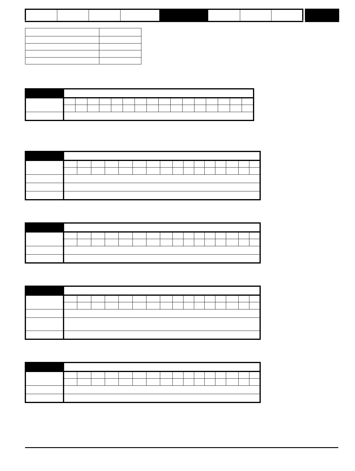
Full scale voltage measurement and the over voltage trip level are defined by DC_VOLTAGE_MAX. However, the maximum level of the low voltage
DC should not normally exceed 90% of this value to avoid spurious over voltage trips.
The drive thermal model system normally controls the fan speed, however the fan can be forced to operate at full speed if this parameter is set to 1.
When this is set to 1 the fan remains at full speed until 10s after this parameter is set to zero.
When the drive is in the UV state the fan always runs at minimum.
This parameter defines the nominal supply voltage when operating in low voltage mode. The parameter is used to define the braking IGBT switching
threshold and the over voltage trip level for low voltage battery mode (see Pr 6.44).
Digitax ST has a diode rectifier input stage with no direct monitoring system. Mains loss and phase loss detection is derived from the DC bus voltage.
This parameter has no effect.
The mains loss detection level can be adjusted using this parameter. If the value is reduced below the default value the default value is used by the
drive. If the level is set too high so that mains loss detection becomes active under normal operating conditions the motor will coast to a stop.
If Pr 6.49 is zero the module number is stored in the module number and trip time log. If this parameter is one, either the powered-up clock or run time
clock is stored in the module number and trip time log as defined by Pr 6.28. It should be noted that changing this parameter clears the trip, and
module number and trip time logs.
Voltage level
DC_VOLTAGE_MAX Pr 6.46 x 1.45
Braking IGBT threshold voltage Pr 6.46 x 1.325
Under voltage trip level 36V
Restart voltage level after UV trip 40V
6.45 Force cooling fan to run at full speed
Coding
Bit SP FI DE TE VM DP ND RA NC NV PT US RW BU PS
111
Update rate Background read
6.46 Nominal low voltage DC supply
Coding
Bit SP FI DE TE VM DP ND RA NC NV PT US RW BU PS
11 1 1
Range 48 to 72V
Default 48
Update rate Background read
6.47 Disable mains/phase loss detection from input rectifier
Coding
Bit SP FI DE TE VM DP ND RA NC NV PT US RW BU PS
111
Default 0
Update rate Background read
6.48 Mains loss ride through detection level
Coding
Bit SP FI DE TE VM DP ND RA NC NV PT US RW BU PS
11 111
Range 0 to DC_VOLTAGE_SET_MAX V
Default
200V rated drive 205
400V rated drive 410
Update rate Background read
6.49 Disable multi-module drive module number storing on trip
Coding
Bit SP FI DE TE VM DP ND RA NC NV PT US RW BU PS
111
Default 0
Update rate Background read