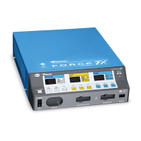
Power Supply/RF Board
4-22 Force FX Electrosurgical Generator C Service Manual
Capacitors C3, C10, C11, and C22 are an energy storage reservoir for the DC/DC
switcher. C29 is a high frequency bypass filter. Bleeder resistors R5 and R6 discharge the
capacitors when the AC line is disconnected or the power switch is turned off.
DC/DC Switching Regulator
The DC/DC switching regulator is a buck derived, pulse width modulated (PWM)
transformer. It is an isolated, fixed frequency, full bridge converter. The PWM IC (U5) is
used in the voltage mode. The output of the regulator is adjustable from approximately
zero (0) to 180 Vdc.
The full bridge consists of four power MOSFETs (Q1, Q3, Q4, and Q5) that operate at AC
line potential. Transistors Q3 and Q5 are on while Q1 and Q4 are off, and the reverse. In
this manner, power signals to the power transformer are bidirectional, or push-pull.
This allows full utilization of the transformer core magnetization capability. Regulation is
achieved by modulating the time that each MOSFET pair is on. Capacitor C32 in series
with the power transformer T3 primary prevents DC flux imbalance.
A snubber circuit (C27 and R31) absorbs leakage energy spikes. Another snubber circuit
(C49 and R51) reduces spikes due to reverse recovery of the output bridge rectifier.
The gate driver circuitry for each MOSFET is transformer-coupled through T1 to provide
AC line isolation. It consists of a dual MOSFET driver (U3) and various damping resistors.
Resistors R12, R18, R21, and R26 minimize turn-off oscillations. Resistors R22 and R23
damp ringing due to parasitic inductances in T1. Blocking capacitors C24 and C25
prevent DC flux imbalance in T1.
Note: T1 consists of two transformers electrically and magnetically isolated from each
other but assembled into the same package. T1A and T1B form one transformer; T1C
and T1D form the other.
The output of the power transformer is full wave rectified by a high voltage diode bridge
(CR10, CR13, CR19, and CR23). L1, C33, and C35 filter the rectified power signal. The
regulated DC output from this supply is the input to the RF stage of the generator.
The SYS_ECON signal from the microcontroller controls the output voltage level. This 0 to
5 Vdc signal sets the reference for the PWM control loop.
An external op-amp (U7B) is used for gain and integration, because common mode
voltage limitations in U5’s internal op-amp preclude its use over the full range of 0 to 5 V.
The internal op-amp is connected as a follower.
SYS_ECON is compared to the feedback voltage from the output divider (R34, R35, and
R49), and an error signal (ECON) is sent to the PWM microcontroller. In addition to the
error signal, U7B and the associated R-C networks provide lead-lag loop compensation to
increase the bandwidth of the regulator beyond that of the output L-C filter.
Note: U7A is used for random gain switching in the Spray mode and is configured for
unity gain in all other modes.