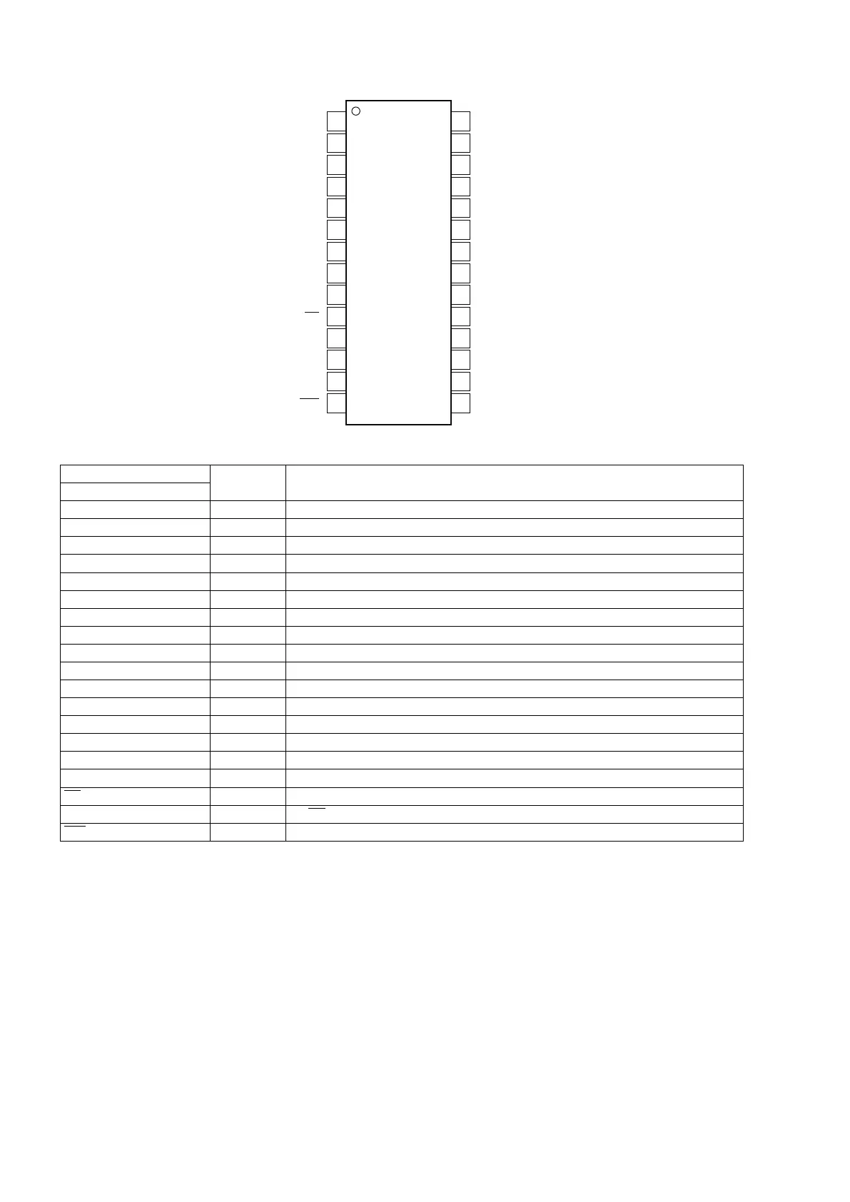
214
PCM1795 (DIGITAL : U0403, U0404, U0405, U0406, U0407, U0408, U0409)
ZEROL
ZEROR
MSEL
LRCK
DATA
BCK
SCL
DGND
V
DD
MS
MDI
MC
MDO
RST
V 2L
CC
AGND3L
IL
OUT
I L+
OUT
AGND2
V1
CC
COM
COM
I
REF
AGND1
IR
OUT
I R+
OUT
AGND3R
V 2R
CC
1
2
3
4
5
6
7
8
9
10
11
12
13
14
28
27
26
25
24
23
22
21
20
19
18
17
16
15
PCM1795
www.ti.com
........................................................................................................................................................................................................ SLES248 – MAY 2009
DB PACKAGE
SSOP-28
(TOP VIEW)
Table 1. TERMINAL FUNCTIONS
TERMINAL
NAME NO. I/O DESCRIPTION
AGND1 19 — Analog ground (internal bias)
AGND2 24 — Analog ground (internal bias)
AGND3L 27 — Analog ground (left channel DACFF)
AGND3R 16 — Analog ground (right channel DACFF)
BCK 6 I Bit clock input
(1)
DATA 5 I Serial audio data input
(2)
DGND 8 — Digital ground
I
OUT
L+ 25 O Left channel analog current output+
I
OUT
L– 26 O Left channel analog current output–
I
OUT
R+ 17 O Right channel analog current output+
I
OUT
R– 18 O Right channel analog current output–
I
REF
20 — Output current reference bias pin
LRCK 4 I Left and right clock (f
S
) input
(2)
MC 12 I Mode control clock input
(2)
MDI 11 I Mode control data input
(2)
MDO 13 I/O Mode control readback data output
(3)
MS 10 I/OI Mode control chip-select input
(4)
; active low
MSEL 3 I I
2
C/SPI select
(2)
; active low SPI select
RST 14 I Reset
(2)
; active low
(1) Schmitt-trigger input, 5-V tolerant.
(2) Schmitt-trigger input, 5-V tolerant.
(3) Schmitt-trigger input and output. 5-V tolerant input. In I
2
C mode, this pin becomes an open-drain 3-state output; otherwise, this pin is a
CMOS output.
(4) Schmitt-trigger input and output. 5-V tolerant input and CMOS output.
Copyright © 2009, Texas Instruments Incorporated Submit Documentation Feedback 7
Product Folder Link(s): PCM1795
 Loading...