215
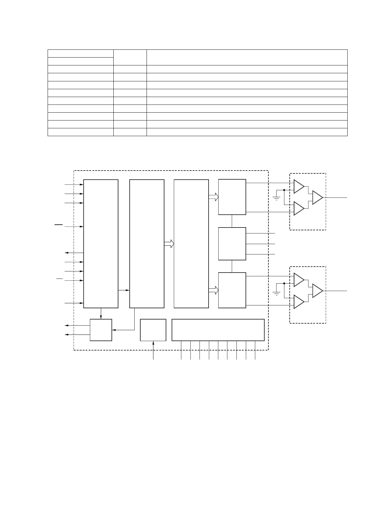
PCM1795 Block Diagram
PCM1795
SLES248–MAY 2009........................................................................................................................................................................................................
www.ti.com
Table 1. TERMINAL FUNCTIONS (continued)
TERMINAL
NAME NO. I/O DESCRIPTION
SCK 7 I System clock input
(2)
V
CC
1 23 — Analog power supply, 5 V
V
CC
2L 28 — Analog power supply (left channel DACFF), 5 V
V
CC
2R 15 — Analog power supply (right channel DACFF), 5 V
V
COM
L 22 — Left channel internal bias decoupling pin
V
COM
R 21 — Right channel internal bias decoupling pin
V
DD
9 — Digital power supply, 3.3 V
ZEROL 1 I/O Zero flag for left channel
(4)
ZEROR 2 I/O Zero flag for right channel
(4)
8 Submit Documentation Feedback Copyright © 2009, Texas Instruments Incorporated
Product Folder Link(s): PCM1795
PowerSupply
RST
SCK
Advanced
Segment
DAC
Modulator
I
OUT
L+
I
OUT
L
I
OUT
R
I
OUT
R+
Bias
andV
REF
V
COM
L
V
COM
R
AGND2
V
DD
V
CC
1
V
CC
2L
V
CC
2R
AGND1
I/V andFilter
x8
Oversampling
DigitalFilter
and
FunctionControl
Audio
DataInput
I/F
LRCK
BCK
D ATA
MDO
MDI
MC
MS
AGND3L
AGND3R
DGND
Current
Segment
DAC
I
REF
V
OUT
L
I/VandFilter
V
OUT
R
Function
ControlI/F
MSEL
Zero
Detect
ZEROL
ZEROR
System
Clock
Manager
Current
Segment
DAC
PCM1795
SLES248–MAY 2009........................................................................................................................................................................................................
www.ti.com
6 Submit Documentation Feedback Copyright © 2009, Texas Instruments Incorporated
Product Folder Link(s): PCM1795
 Loading...