.......................................................................
LA-3500
...
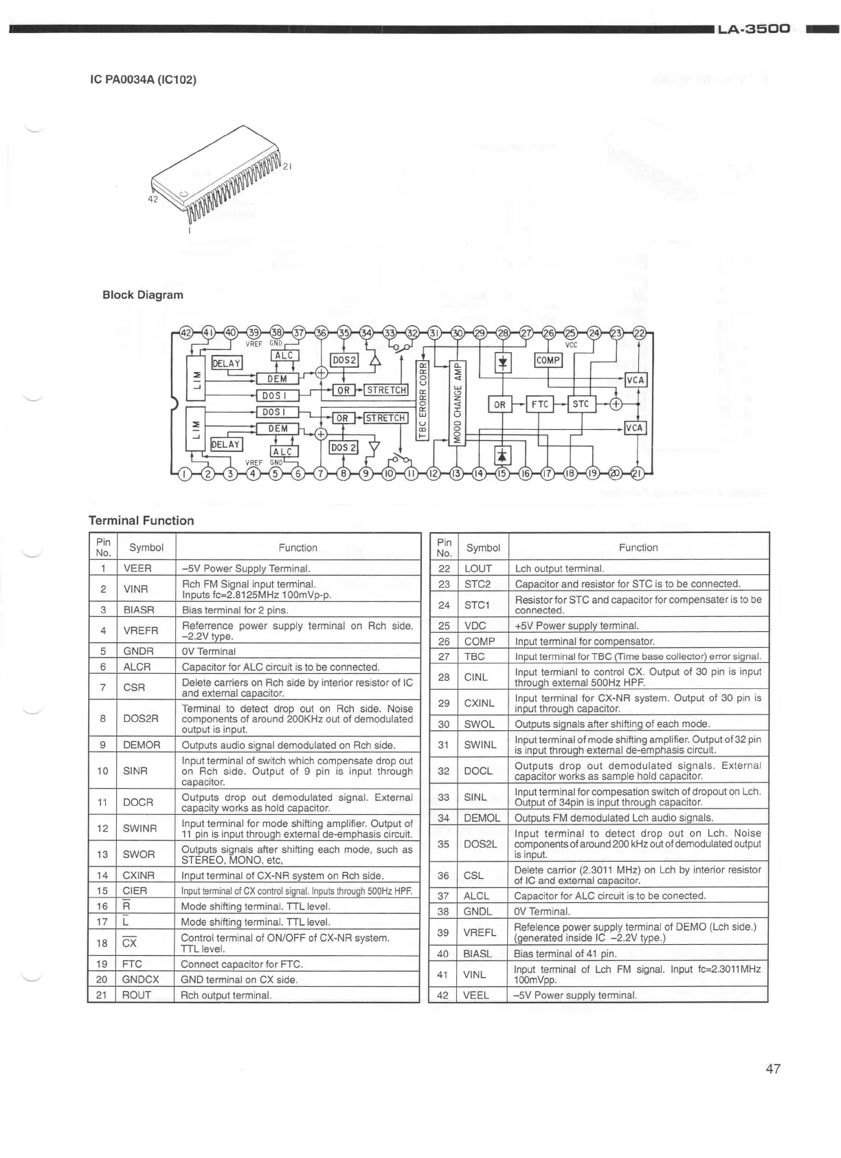
IC PA0034A (IC102)
2 1
Block Diagram
Terminal Function
P
in
Symbol
Function
No.
P
in
Symbol
Function
No.
1
VEER
-5V
Power Supply Term inal.
22 LOUT
Leh
outputterminal.
2
VINR
Reh
FM
Signal input terminal.
Inputs
fc=2.8125MHz 100mVp-p.
3
BIASR
Bias te
rm
inal for 2 pins.
23
STC2
Capacitor and resistor for STC is to be connected.
24
STC1
Resistor for STC and capacitor for compensater
is
to be
connected.
VREFR
Referrence power
supply terminal
on
Reh
side.
4
-2
.
2Vtype
.
25
voe +5V Power supply terminal.
26
COMP
Input terminal
for compensator.
5
GNDR
OVTerminal
27 TBC
Input terminal for TBC
(llme
base collector) error signal.
6 ALCR Capacitor for ALC circuit
is
to be connected.
7
CSR
Delete
carriers
on
Reh
side
by
interior resistor
of
IC
and external capacitor.
Terminal to detect drop out
on
Reh
side. Noise
28
CINL
Input termianl
to control CX. Output of 30 pin
is
input
through
external 500Hz
HPF.
29 CXINL
Input terminal
for CX-NR system . Output of 30 pin
is
input through capacitor.
8
DOS2R
components of around 200KHz out of demodulated
output is input.
30 SWOL
Outputs signals
after shifting of each mode .
9
DEM
OR
Outputs
audio signal demodulated
on
Reh
side.
31
SWINL
Input terminal
of mode shifting amplifier. Output of 32 pin
is
input through external de-emphasis
c1rcu1t.
Input terminal of switch which compensate drop out
10 SINR
on Reh side. Output
of
9 pin is input through
capacitor.
11
DOCR
Outputs
drop out demodulated signal. External
capacity works as hold capacitor.
32
DOCL
Outputs
drop
out
demodulated
si~nals.
External
capacitor works as sample hold capacitor.
33
SINL
Input terminal
for compesation switch o_f dropout
on
Leh.
Output of 34pin
is
input through capacitor.
12
SWINR
Input terminal
for mode shifting amplifier. Output of
11
pin is input through external de-emphasis circuit.
13
SWOR
Outputs signals
after shifting each mode, such as
STEREO, MONO, etc,
34
DEMOL
Outputs
FM
demodulated
Leh
audio signals.
Input
terminal
to
detect
drop
out
on Leh. Noise
35
DOS2L
components of around 200 kHz out of demodulated output
is
input.
14
CXINR Input terminal of CX-NR system
on
Reh
side.
36
CSL
Delete
carrier (2.3011 MHz)
on
Leh
by interior resistor
of
IC and external capacitor.
15
GIER
Input
t
erminal
of
CX
control
signal.
Inputs
through
SOOHz
HPF
.
37 ALCL
Capacitor for ALC circuit
is
to be conected.
16
R
Mode shifting
terminal. TTL level.
38 GNDL
OV
Terminal.
17 L Mode shifting terminal. TTL level.
-
Control terminal of ON/OFF of CX-NR system.
18
ex
TTL
level.
39
VREFL
Refelence power supply terminal of DEMO (Leh side.)
(generated inside
IC - 2.2V type.)
40 BIASL Bias terminal
of
41
pin .
19 FTC Connect capacitor for FTC.
20 GNDCX GND terminal on CX side.
41
VINL
Input terminal
of
Leh
FM
signal. Input fc=2.
3011
MHz
100mVpp.
21
ROUT
Reh
output terminal. 42 VEEL
-5V
Power supply terminal.
47