Mapping of I/O Signals
▲
■■■■■■■■■■■■■■■■■■■■■■■■■■■■■■■■■■■■■■■■■■■■■■■■■■■■■■■■■■■■■■■■■■■■■■■■■■■■■■■■■■■■■■■■■■■■■■■■
DS1104 Hardware Installation and Configuration March 2004
I■■■■■■■■■■■■■
▼
106
■■■■■■■■■■■■■■■▼
Slave DSP PWM Signal Generation (PWM, PWM3, PWMSV)
• TTL output voltage range
• Output current range: ±13 mA
• I/O circuit and further electrical characteristics: see Slave DSP Digital I/O on page 142
ST2PWM * DS1104SL_DSP_PWM Ch 1 See Slave DSP PWM
Generation in the DS1104
RTLib Reference
Ch 1 P1 23 P1B 21 CP18 5
SPWM7 * Ch 2 Ch 2 P1 31 P1B 6 CP18 10
SPWM8 * Ch 3 Ch 3 P1 29 P1B 22 CP18 29
SPWM9 * Ch 4 Ch 4 P1 27 P1B 38 CP18 11
SPWM1 * DS1104SL_DSP_PWM3 /
DS1104SL_DSP_PWMSV
Phase 1 See Slave DSP PWM3
Generation /
Slave DSP PWMSV Generation
in the DS1104 RTLib Reference
Phase 1 P1 32 P1A 6 CP18 7
SPWM3 * Phase 2 Phase 2 P1 28 P1A 38 CP18 8
SPWM5 * Phase 3 Phase 3 P1 24 P1A 21 CP18 9
SPWM2 Phase 1
(inverted)
Phase 1
(inverted)
P1 30 P1A 22 CP18 26
SPWM4 Phase 2
(inverted)
Phase 2
(inverted)
P1 26 P1A 5 CP18 27
SPWM6 Phase 3
(inverted)
Phase 3
(inverted)
P1 22 P1A 37 CP18 28
Slave DSP Square-Wave Signal Generation (D2F)
• TTL output voltage range
• Output current range: ±13 mA
• I/O circuit and further electrical characteristics: see Slave DSP Digital I/O on page 142
SPWM1 * DS1104SL_DSP_D2F Ch 1 See Square Wave Signal
Generation (D2F) in the
DS1104 RTLib Reference
Ch 1 P132 P1A6 CP187
SPWM3 * Ch 2 Ch 2 P1 28 P1A 38 CP18 8
SPWM5 * Ch 3 Ch 3 P1 24 P1A 21 CP18 9
ST2PWM * Ch 4 Ch 4 P1 23 P1B 21 CP18 5
Slave DSP PWM Signal Measurement (PWM2D)
• TTL input voltage range
• I/O circuit and further electrical characteristics: see Slave DSP Digital I/O on page 142
SCAP1 * DS1104SL_DSP_PWM2D Ch 1 See Slave DSP PWM
Measurement (PWM2D) in the
DS1104 RTLib Reference
Ch 1 P1 18 P1A 20 CP18 2
SCAP2 * Ch 2 Ch 2 P1 16 P1A 36 CP18 21
SCAP3 * Ch 3 Ch 3 P1 14 P1A 3 CP18 3
SCAP4 * Ch 4 Ch 4 P1 12 P1A 19 CP18 22
Slave DSP Square-Wave Signal Measurement (F2D)
• TTL input voltage range
• I/O circuit and further electrical characteristics: see Slave DSP Digital I/O on page 142
SCAP1 * DS1104SL_DSP_F2D Ch 1 See Square Wave Signal
Measurement (F2D) in the
DS1104 RTLib Reference
Ch 1 P1 18 P1A 20 CP18 2
SCAP2 * Ch 2 Ch 2 P1 16 P1A 36 CP18 21
SCAP3 * Ch 3 Ch 3 P1 14 P1A 3 CP18 3
SCAP4 * Ch 4 Ch 4 P1 12 P1A 19 CP18 22
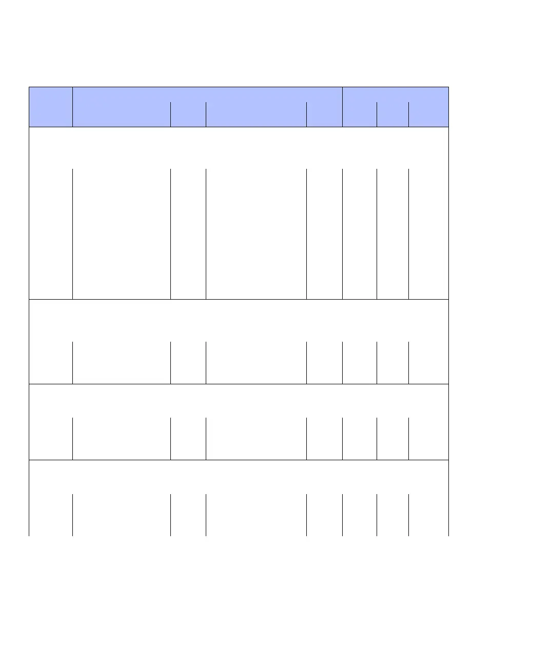
Signal
Channel/Bit Numbers of Related RTI Blocks/RTLib Functions I/O Pin on …
Related RTI Block(s)
Ch/Bit
(RTI)
Related RTLib Functions
Ch/Bit
(RTLib)
DS1104
Sub-D
Conn.
CP/CLP