II CORE BLOCK: BCU (Bus Control Unit)
B-II-4-28 EPSON S1C33L03 FUNCTION PART
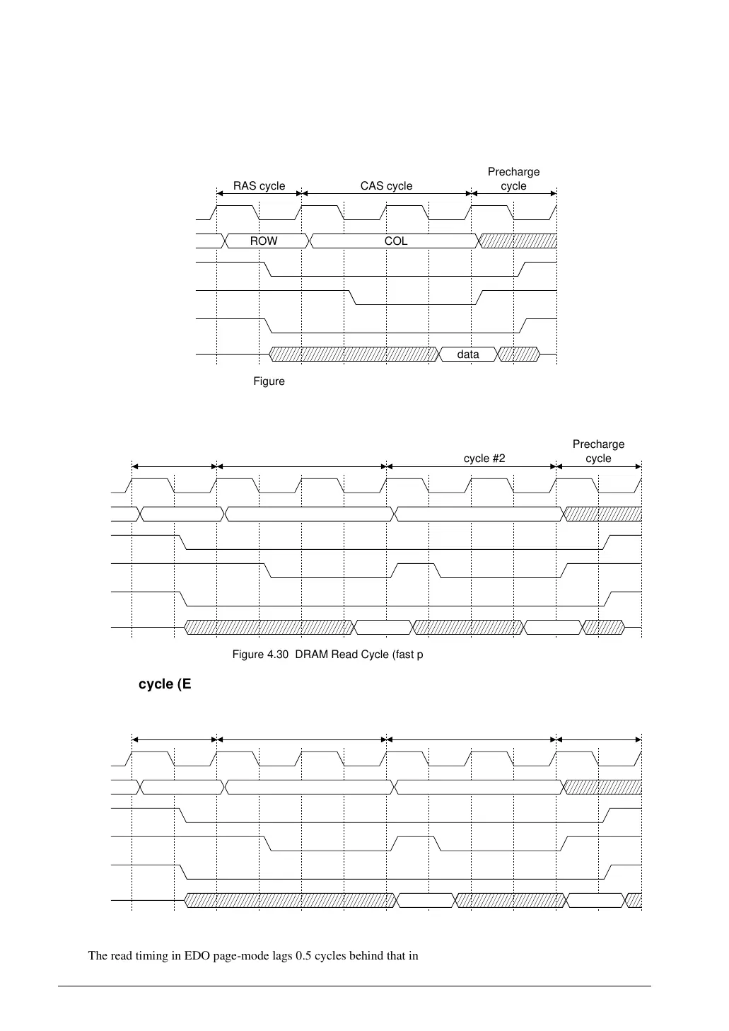
DRAM Read/Write Cycles
The following shows the basic bus cycles of DRAM.
The DRAM interface does not accept wait cycles inserted via the #WAIT pin.
DRAM random read cycle
Example: RAS: 1 cycle; CAS: 2 cycles; Precharge: 1 cycle
BCLK
A[11:0]
#RASx
#HCAS/
#LCAS
#RD
D[15:0]
;;;;;;;;;;;;;
;;;;;;;;;;;;;
ROW COL
data
RAS cycle CAS cycle
Precharge
cycle
Figure 4.29 DRAM Random Read Cycle
DRAM read cycle (fast page mode)
Example: RAS: 1 cycle; CAS: 2 cycles; Precharge: 1 cycle
BCLK
A[11:0]
#RASx
#HCAS/
#LCAS
#RD
D[15:0]
;;;;;;;;;;;;;
;;;;;;;;;;;;;
ROW COL #1 COL #2
data
data
RAS cycle CAS cycle #1 CAS cycle #2
Precharge
cycle
Figure 4.30 DRAM Read Cycle (fast page mode)
DRAM read cycle (EDO page mode)
Example: RAS: 1 cycle; CAS: 2 cycles; Precharge: 1 cycle
BCLK
A[11:0]
#RASx
#HCAS/
#LCAS
#RD
D[15:0]
;;;;;;;;;;;;;;;;
;;;;;;;;;;;;;;;;
ROW COL #1 COL #2
data
data
RAS cycle CAS cycle #1 CAS cycle #2
Precharge
cycle
Figure 4.31 DRAM Read Cycle (EDO page mode)
The read timing in EDO page-mode lags 0.5 cycles behind that in fast page mode.
 Loading...