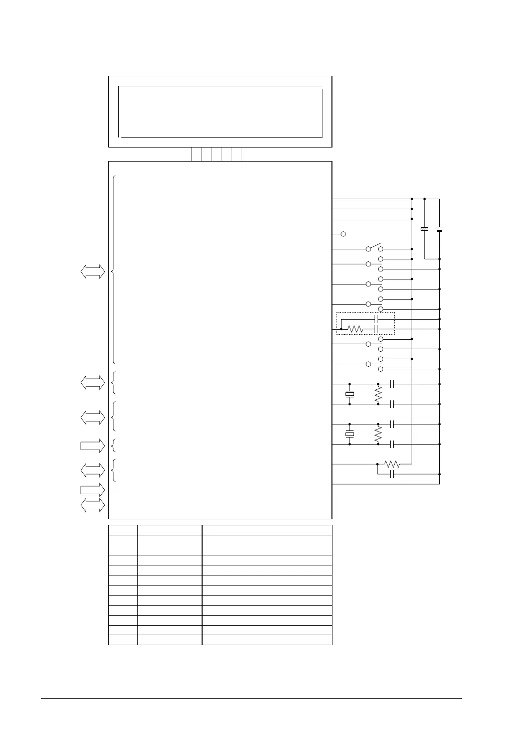
6 BASIC EXTERNAL WIRING DIAGRAM
A-68 EPSON S1C33L03 PRODUCT PART
6 Basic External Wiring Diagram
S1C33L03
[The potential of the substrate
(back of the chip) is V
SS.]
External
Bus
HSDMA
Serial I/O
A/D input
Input
I/O
Timer
input/output
X'tal1
C
G1
CD1
Rf1
X'tal2
CR
C
G2
CD2
Rf2
R1
C1
C2
Crystal oscillator
Gate capacitor
Drain capacitor
Feedback resistor
Crystal oscillator
Ceramic oscillator
Gate capacitor
Drain capacitor
Feedback resistor
Resistor
Capacitor
Capacitor
32.768 kHz, CI(Max.) = 34 kΩ
10 pF
10 pF
10 MΩ
33 MHz (Max.)
33 MHz (Max.)
10 pF
10 pF
1 MΩ
4.7 kΩ
100 pF
5 pF
Note: The above table is simply an example, and is not guaranteed to work.
∗1: When the PLL is not used,
leave the PLLC pin open.
VDD
VDDE
AVDDE
DSIO
ICEMD
EA10MD0
EA10MD1
#X2SPD
PLLC
PLLS0
PLLS1
OSC3
OSC4
OSC1
OSC2
#RESET
V
SS
C
D2
3.3V
X'tal2
or
CR
Rf
2
A[23:0]
D[15:0]
#RD
#EMEMRD
#DRD
#GARD
#GAAS
#WRL/#WR/#WE
#WRH/#BSH
#DWE/#SDWE
#HCAS/#SDCAS
#LCAS/#SDRAS
#CExx/#RASx/#SDCEx
SDA10
SDCKE
HDQM/LDQM
#CE10EX
#WAIT
BCLK
#BUSREQ
#BUSACK
#BUSGET
#NMI
#DMAREQx
#DMAACKx
#DMAENDx
SINx
SOUTx
#SCLKx
#SRDYx
#ADTRG
ADx
EXCLx
TMx
T8UFx
Kxx
Pxx
C
G2
C
2
C
1
R
1
∗1
+
C
D1
X'tal1 Rf
1
C
G1
FPDAT[7:0]
FPSHIFT
FPFRAME
FPLINE
DRDY
LCDPWR
LCD panel