V DMA BLOCK: HSDMA (High-Speed DMA)
S1C33L03 FUNCTION PART EPSON B-V-2-13
A-1
B-V
HSDMA
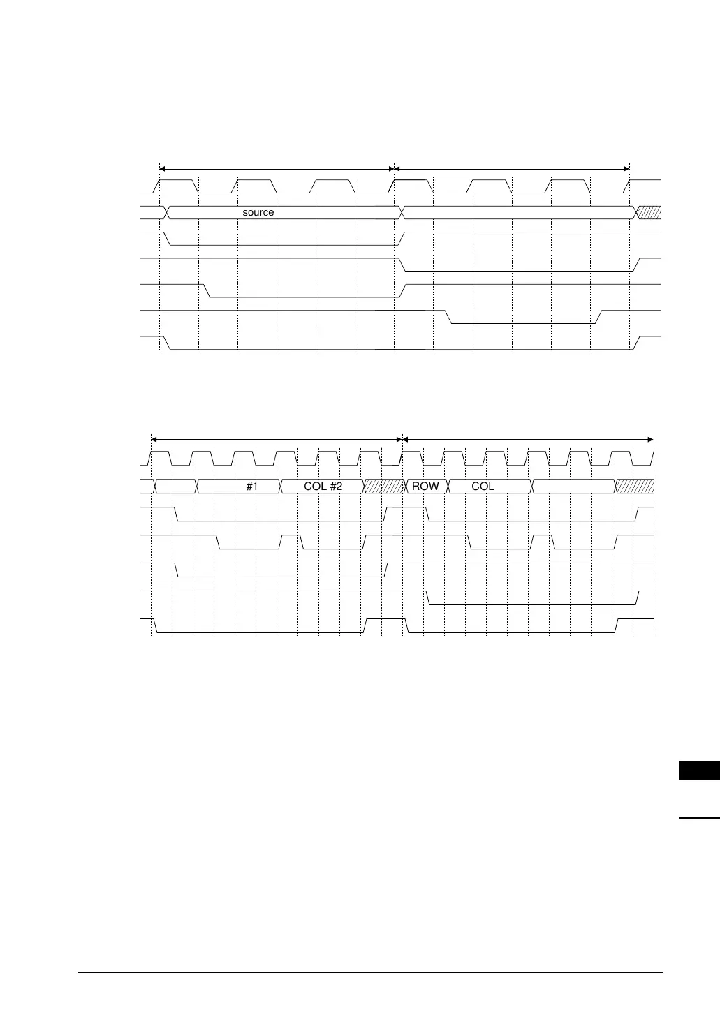
Timing Chart
Dual-address mode
(1) SRAM
Example: When 2 (RD)/1 (WR) wait cycles are inserted
BCLK
A[23:0]
#CE(src)
#CE(dst)
#RD
#WRH/#WRL
#DMAEND
source address destination address
Read cycle Write cycle
Figure 2.6 #DMAEND Signal Output Timing (SRAM)
(2) DRAM
Example: Page mode, RAS: 1 cycle; CAS: 2 cycles; Precharge: 1 cycle
BCLK
A[11:0]
#RASx
#HCAS/
#LCAS
#RD
#WR
#DMAEND
ROW COL #1 COL #2 ROW COL #1 COL #2
Read cycle Write cycle
Figure 2.7 #DMAEND Signal Output Timing (DRAM)
 Loading...