IV ANALOG BLOCK: A/D CONVERTER
S1C33L03 FUNCTION PART EPSON B-IV-2-9
A-1
B-IV
A/D
I/O Memory of A/D Converter
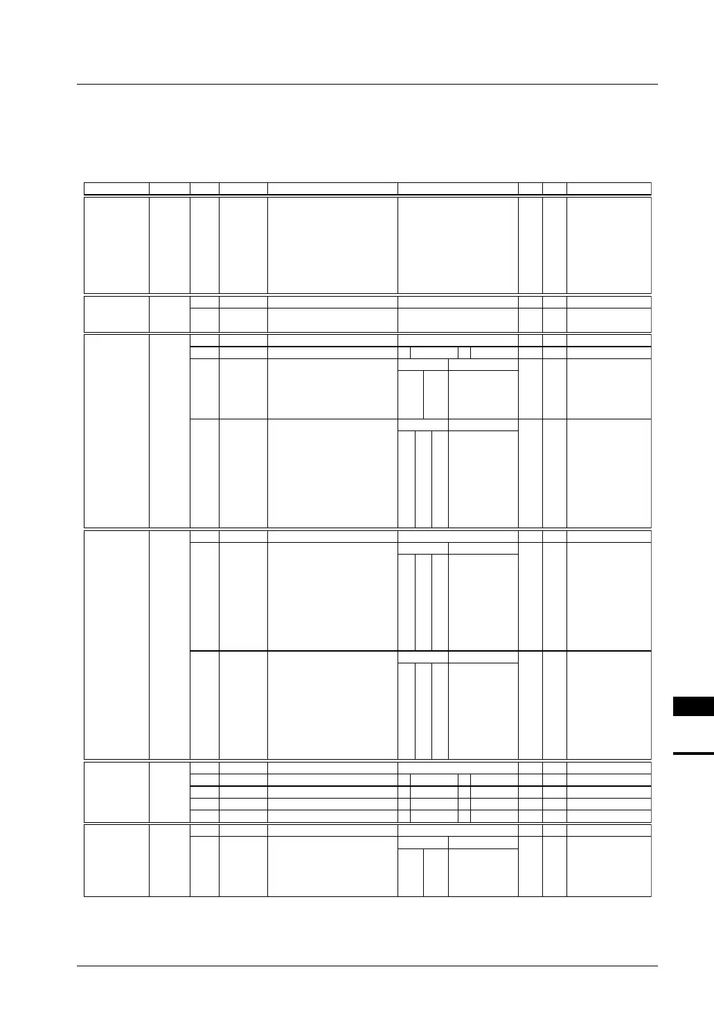
Table 2.6 shows the control bits of the A/D converter.
For details on the I/O memory of the prescaler used to set clocks, refer to "Prescaler". For details on the I/O
memory of the programmable timers used for a trigger, refer to "8-Bit Programmable Timers" or "16-Bit
Programmable Timers".
Table 2.6 Control Bits of A/D Converter
NameAddressRegister name Bit Function Setting Init. R/W Remarks
ADD7
ADD6
ADD5
ADD4
ADD3
ADD2
ADD1
ADD0
D7
D6
D5
D4
D3
D2
D1
D0
A/D converted data
(low-order 8 bits)
ADD0 = LSB
0x0 to 0x3FF
(low-order 8 bits)
0
0
0
0
0
0
0
0
R0040240
(B)
A/D conversion
result (low-
order) register
0x0 to 0x3FF
(high-order 2 bits)
––
ADD9
ADD8
D7–2
D1
D0
–
A/D converted data
(high-order 2 bits) ADD9 = MSB
–
0
0
–
R
0 when being read.0040241
(B)
A/D conversion
result (high-
order) register
–
MS
TS1
TS0
CH2
CH1
CH0
D7–6
D5
D4
D3
D2
D1
D0
–
A/D conversion mode selection
A/D conversion trigger selection
A/D conversion channel status
1
1
0
0
1
0
1
0
TS[1:0]
–
Trigger
#ADTRG pin
8-bit timer 0
16-bit timer 0
Software
1
1
1
1
0
0
0
0
1
1
0
0
1
1
0
0
1
0
1
0
1
0
1
0
CH[2:0] Channel
AD7
AD6
AD5
AD4
AD3
AD2
AD1
AD0
–
0
0
0
0
0
0
–
R/W
R/W
R
0 when being read.0040242
(B)
1 Continuous 0 Normal
A/D trigger
register
–
1
1
1
1
0
0
0
0
1
1
0
0
1
1
0
0
1
0
1
0
1
0
1
0
CE[2:0] End channel
AD7
AD6
AD5
AD4
AD3
AD2
AD1
AD0
1
1
1
1
0
0
0
0
1
1
0
0
1
1
0
0
1
0
1
0
1
0
1
0
CS[2:0] Start channel
AD7
AD6
AD5
AD4
AD3
AD2
AD1
AD0
–
CE2
CE1
CE0
CS2
CS1
CS0
D7–6
D5
D4
D3
D2
D1
D0
–
A/D converter
end channel selection
A/D converter
start channel selection
–
0
0
0
0
0
0
–
R/W
R/W
0 when being read.0040243
(B)
A/D channel
register
–
ADF
ADE
ADST
OWE
D7–4
D3
D2
D1
D0
–
Conversion-complete flag
A/D enable
A/D conversion control/status
Overwrite error flag
– –
0
0
0
0
–
R
R/W
R/W
R/W
0 when being read.
Reset when ADD is read.
Reset by writing 0.
0040244
(B)
A/D enable
register
1 Enabled 0 Disabled
1 Completed 0
Run/Standby
1 Start/Run 0 Stop
1 Error 0 Normal
–
ST1
ST0
D7–2
D1
D0
–
Input signal sampling time setup
–
1
1
0
0
1
0
1
0
ST[1:0] Sampring time
9 clocks
7 clocks
5 clocks
3 clocks
–
1
1
–
R/W
0 when being read.
Use with 9 clocks.
0040245
(B)
A/D sampling
register
 Loading...