3–4 D485 MODBUS TO DEVICENET CONVERTER – USER GUIDE
DATA EXCHANGE
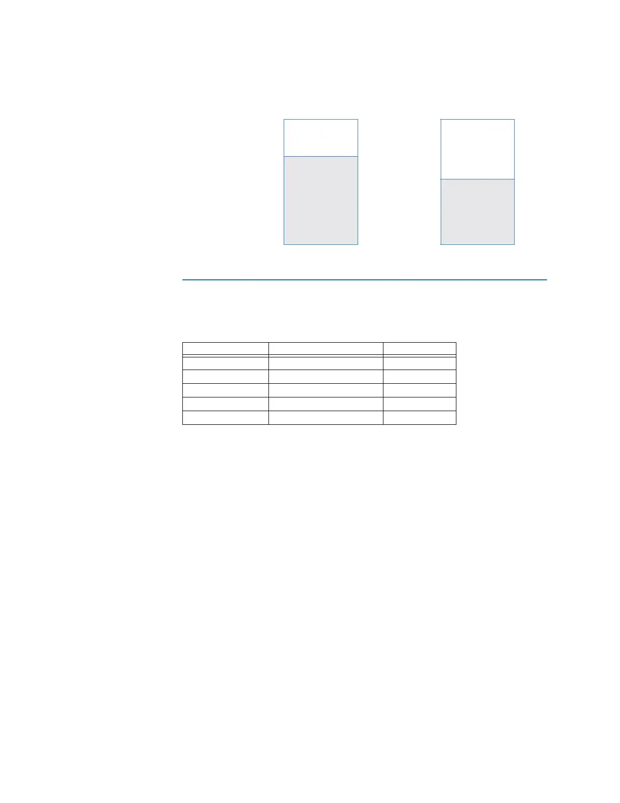
For example, when using an input I/O size of 50 and an output I/O size of 60, the input and
output data areas will be allocated as follows:
Figure 3-4: I/O data area example
Memory Map
MEMORY LOCATIONS When configuring the sub-network, use the memory locations shown below:
• Status register (0x0000 to 0x0001): If enabled, this register occupies the first two
bytes in the input data area. For more information, see Control and status registers on
page 8–1.
• Input data area (0x002 to 0x01FF): This area holds data that should be sent to the
fieldbus (see the status and control registers).
• Control register (0x0200 to 0x0201): If enabled, these register occupies the first two
bytes in the output data area. For more information, see Control and status registers
on page 8–1.
• Output data area (0x0202 to 0x03FF): This area holds data received from the fieldbus.
Data cannot be written to this area.
• General data Area (0x0400 to 0x07FB): This data cannot be accessed from the
fieldbus, and should be used for transfers between nodes on the Modbus sub-
network, or as a general “scratch pad” for data.
Input data area Output data area
50 bytes
462 bytes
(512 – 50 = 462)
60 bytes
452 bytes
(512 – 60 = 462)
I/O data (input)
I/O data (input)
Explicit data
(input)
Explicit data
(output)
Address Contents Access
0x0000 to 0x0001 Status register read/write
0x0002 to 0x01FF Input data area read/write
0x0200 to 0x0201 Control register read only
0x0202 to 0x03FF Output data area read only
0x0400 to 0x07FB General data area read/write