Contents
ix
5 Regulatory Compliance and Battery Disposal Information
5.1 Regulatory Compliance.......................................................................................................................... 85
5.1.1 Safety Standards .................................................................................................................... 85
5.1.2 European Union Declaration of Conformity Statement ........................................ 86
5.1.3 EMC Regulations .................................................................................................................... 87
5.1.4 e-Standby and ErP Compliance....................................................................................... 90
5.1.5 Regulatory Compliance Marks (Board Level) ............................................................. 91
5.2 Battery Disposal Information .............................................................................................................. 92
Figures
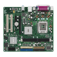
1. Major Board Components (Top)......................................................................................................... 15
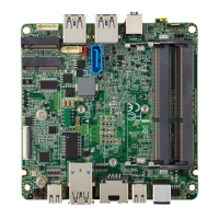
2. Major Board Components (Bottom) ................................................................................................. 17
3. Block Diagram ............................................................................................................................................ 19
4. Memory Channel and SO-DIMM Configuration ........................................................................... 22
5. Flat Panel Connector on Bottom-side of the Board .................................................................. 26
6. Flat Panel Connectors on Top-side of the Board ....................................................................... 27
7. 4-Pin 3.5 mm (1/8 inch) Audio Jack Pin Out ................................................................................ 32
8. LAN Connector LED Locations ............................................................................................................ 34
9. Thermal Solution and Fan Header .................................................................................................... 36
10. Location of the Standby Power LED ................................................................................................. 41
11. Front Panel Connectors ......................................................................................................................... 48
12. Back Panel Connectors .......................................................................................................................... 48
13. Connectors and Headers (Top)........................................................................................................... 49
14. Connectors and Headers (Bottom) ................................................................................................... 50
15. Connection Diagram for the Internal Power Supply Connector ........................................... 58
16. Connection Diagram for Front Panel Header (2.0 mm Pitch) ................................................ 59
17. Low Speed Custom Solutions Header ............................................................................................. 61
18. Connection Diagram for Internal USB 2.0 Dual-Port Header (1.25 mm Pitch) ............... 62
19. Location of the BIOS Security Jumper ............................................................................................ 63
20. Intel MEBX Reset Header ...................................................................................................................... 66
21. Board Dimensions .................................................................................................................................... 67
22. Board Height Dimensions ..................................................................................................................... 68
23. Localized High Temperature Zones ................................................................................................. 71
24. Installation Area of the Thermal Pad ............................................................................................... 72