Connector Pin Assignment RBA-40C™ Banknote Acceptor Section 4
Issue #4119-IGE-01-00 © 2020, JAPAN CASH MACHINE CO., LTD.
4 CONNECTOR PIN ASSIGNMENT
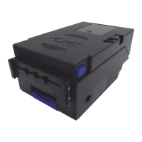
This section provides the pin assignments of the RBA-40C™ Series Banknote Acceptor (RBA-40C).
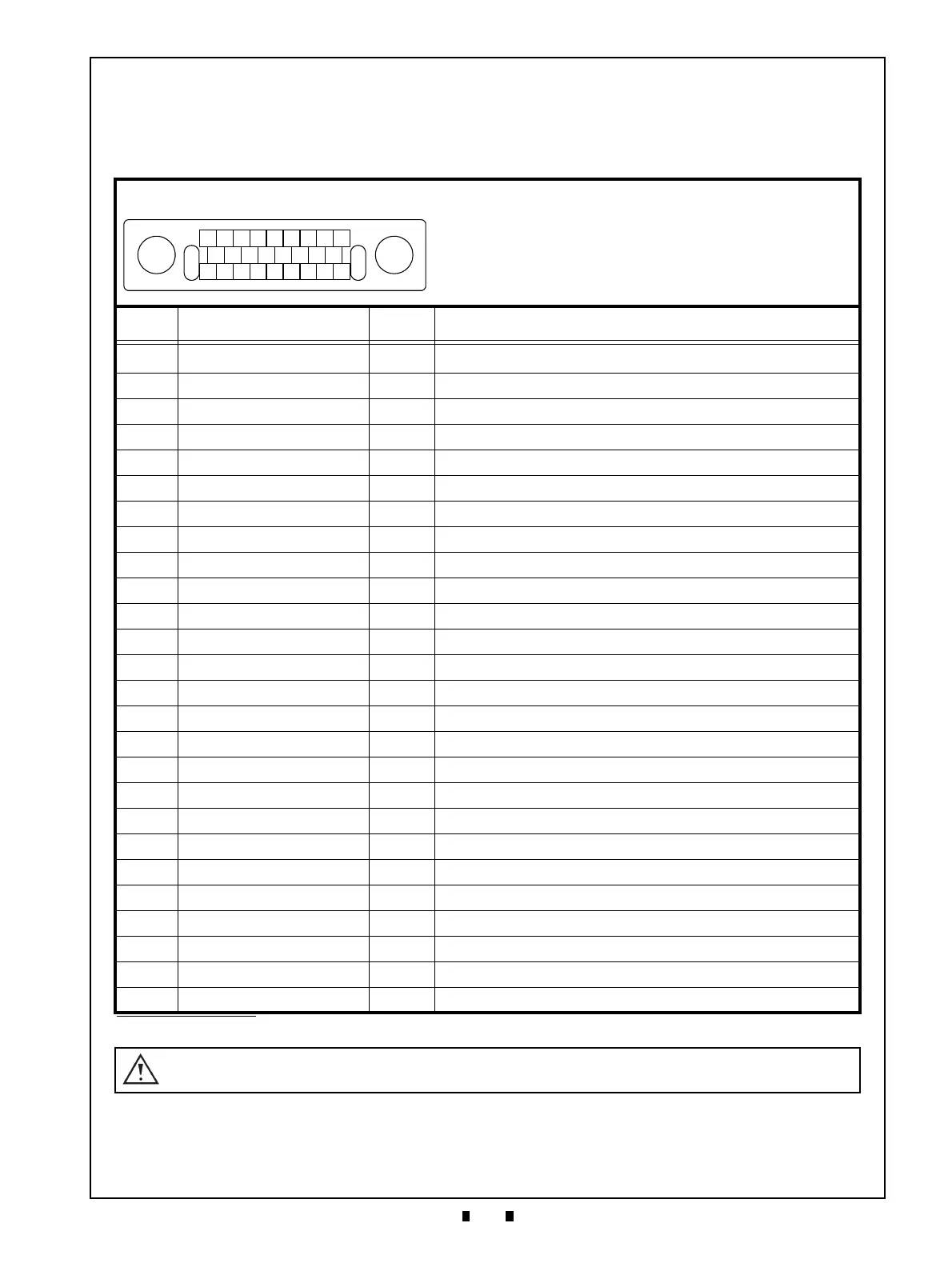
Power Supply Connector Pin Assignment; TTL and Encoder
Table 10 Power Supply Connector Pin Assignments (TTL and Encoder)
Socket (RBA-40C Side): DRA-20PC-FO (JAE)
Contact (RBA-40C Side): D02-22-26P-10000 (JAE)
Socket (MD-100 Side): DRA-20SC-FO (JAE)
Contact (MD-100 Side): D02-22-26S-10000 (JAE)
Recommended Wire: Ul1571 AWG#26
Pin No. Signal Name
I/O
*
*. I/O (input/output) is the terminal as viewed from the Banknote Acceptor.
Function
1
NC -
No Connection
2 NC - No Connection
3 NC - No Connection
4 GND - Ground
5 +5V - 5V DC Power Supply
6 NC - No Connection
7 NC - No Connection
8 NC - No Connection
9 NC - No Connection
10 NC - No Connection
11 NC - No Connection
12 NC - No Connection
13 NC - No Connection
14 NC - No Connection
15 NC - No Connection
16 NC - No Connection
17 NC - No Connection
18 NC - No Connection
19 MD-100_ENC1 OUT MD-100 Encoder Signal 1 (Photointerrupter Emitter Signal)
20 MD-100_ENC2 OUT MD-100 Encoder Signal 2 (Transistor Collector Signal)
21 MD-100_5V IN 5V DC Power Supply
22 NC - No Connection
23 +24V - 24V DC Power Supply
24 TTL-RXD IN TTL Input Signal Line
25 TTL-TXD OUT TTL Output Signal Line
26 GND - Ground
CAUTION: Pin #5 is designed to supply +5V DC power to Pin #21 via the ADP’s PCB.
Do Not use Pin #5 for other purposes to avoid the risk of damage to the Unit.