SECTION
4
THEORY
OF
OPERATION
4.1 INTRODUCTION
4.3.2 Input Buffer Amplifier
This section contains an overall functional description of the
Model 197. Information pertaining to the Model 1978 Battery
Pack option is also included. Detailed schematics and compo-
nent layout drawings are located at the end of this instruction
manual.
The input buffer amplifier provides the necessary isolation
between the input signal and the A/D converter. The
amplifier is a noninverting, low noise, high impedance circuit
with
X1
or
XI0 gain. The amplifier gain is controlled by the
microprocessor and is range and function dependent. Figure
4-3 shows the simplified schematic of the input buffer
amplifier. The gain is XI0 when Qll6 is ON and
X1
when
Q116 is
OFF.
4.2 OVERALL FUNCTIONAL DESCRIPTION
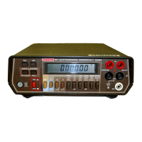
The Model 197 is a
5%
digit DMM with five AC and DC
voltage ranges, seven resistance ranges and six
AC
and DC
current ranges. A simplified block diagram of the Model 197
is shown in Figure 4-1. The heart of the Model 197 is the A/D The Model 197 voltage and current measurements are based
converter that translates the conditioned analog input signal on comparing the unknown signal with an internal 2V
into a form usable by the microcomputer. reference voltage. During each measurement cycle the
unknown is sampled along with a zero measurement and a
2V
reference measurement to compute the unknown voltage.
4.3.3 2v Reference Source
4.3 ANALOG CIRCUITRY
The 2V reference is made up of a highly stable Zener diode
(VRl03), an op-amp and a resistive divider. U109 and R125C,
The following paragraphs contain a description of the input
multiplexer, buffer amplifier, +2V reference and A/D con-
D, and
E
act as a constant CWTent Source to minimize the
verter
circuits.
These circuits
may
be found
on
schematic
diagram number 197-106 located at the end of this manual.
Zener voltage variations. R121D,
E
and
F
is
then used to
divide
down
the
6.4v
to
2v.
4.3.1 Multiplexer
The multiplexer connects one of four signals to the buffer
amplifier: signal, zero, reference and ohms reference. The
multiplexer, shown in Figure 4-2, is made up of 4 JFETs which
are controlled by the microprocessor through U114. The FETs
are driven by drivers U103 and U112. The drivers convert the
digital signals of the microprocessor to signals usable by the
FETs.
Note that the particular
FET
used to sense zero on DCV is
range dependent. This is done
so
that zero may be sensed in a
manner that eliminates the errors due to the
ON
resistances of
Q106 and Ql09.
It
also reduces errors due to leakage current
The output of U109 is buffered by Q122 to form a
+1OV
sup-
Ply.
4.3.4 Input Signal Conditioning
For DCV and ACV the signal conditioning is performed by
R103, R104, R105 and their shunt capacitors. Range switch-
ing is performed by K101, K102, K103, Q105, Q106 and
Ql09. Q107 and
QlO8
are used to sense zero in a manner that
eliminates the errors due to the on resistances of Q106 and
Ql09. The FETs are driven by U112.
The following attenuation is provided:
-
+I
is used on the 200mV and 2V ranges.
+lo
is used on the 2OV range.
of
u102.
+loo
is used on the 2OOV range.
+lo00 is used on the 1000V/750V range.
Ordinarily, FET switching creates transients which could be
seen in the final measurement. These effects are minimized in
the Model 197 through the use of software generated delays
4-
1
Artisan Technology Group - Quality Instrumentation ... Guaranteed | (888) 88-SOURCE | www.artisantg.com