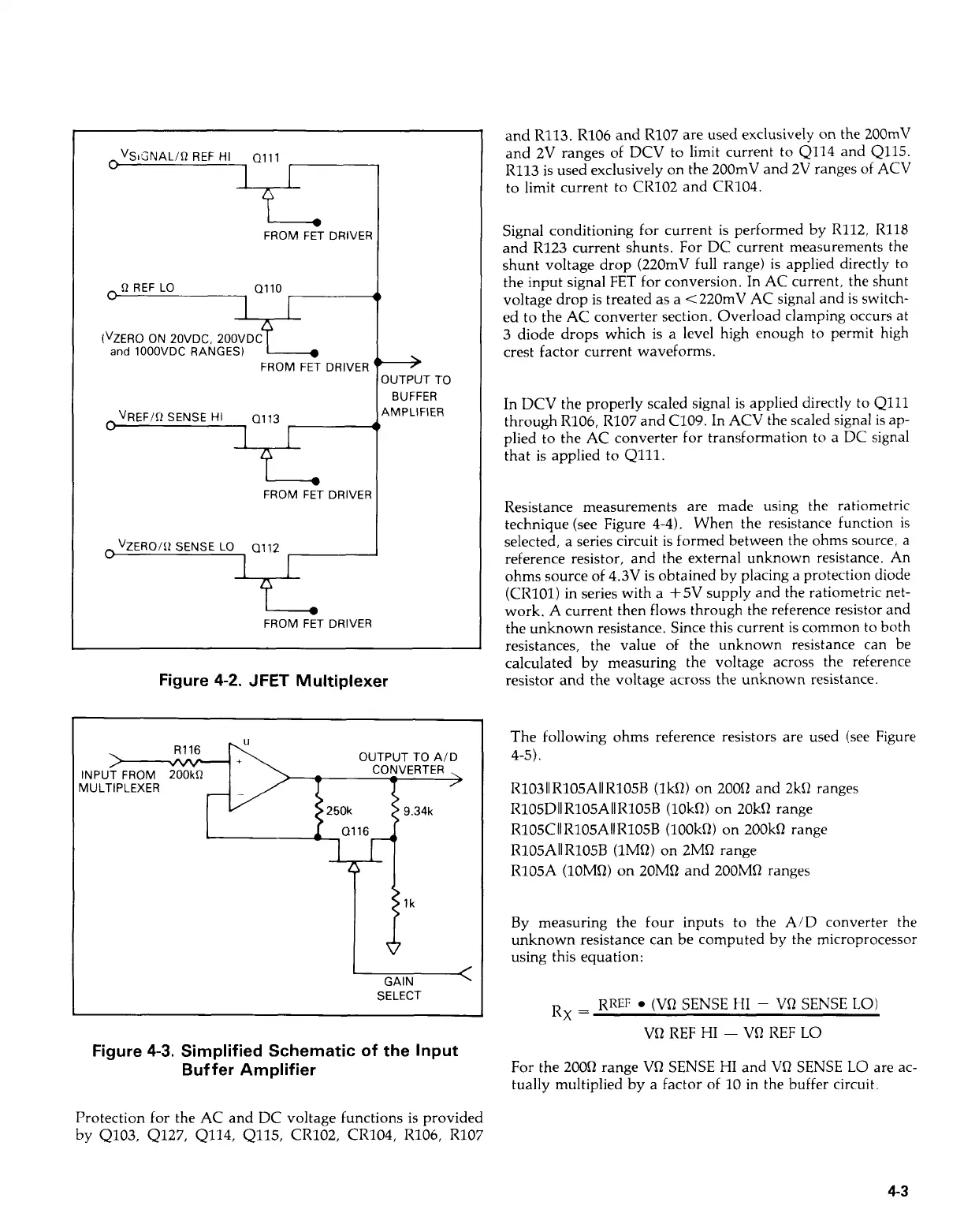
OVS~SNAL/R REF
HI
,
,
.
FROM FET DRIVER
R
REF
LO
Q110
1
I
(VZERO
ON
ZOVDC,
and
lOOOVDC RANGES)
FROM FET DRIVER
VREF~R
SENSE
HI
0113
1
I
f
-
FROM FET DRIVER
+
IUTPUT TO
BUFFER
AMPLIFIER
FROM FET DRIVER
Figure
4-2.
JFET
Multiplexer
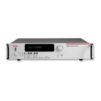
INPU? FROM
MULTIPLEXER
200kR
GAIN
<
SELECT
Figure
4-3.
Simplified Schematic of the Input
Buffer Amplifier
and R113. R106 and R107 are used exclusively on the 200mV
and 2V ranges of
DCV
to limit current to Q114 and Qll5.
R113 is used exclusively on the 200mV and 2V ranges of ACV
to limit current to CR102 and CR104.
Signal conditioning for current is performed by R112, R118
and R123 current shunts. For DC current measurements the
shunt voltage drop (220mV full range) is applied directly to
the input signal FET for conversion. In AC current, the shunt
voltage drop is treated as a <220mV
AC
signal and is switch-
ed to the AC converter section. Overload clamping occurs at
3
diode drops which
is
a level high enough to permit high
crest factor current waveforms.
In DCV the properly scaled signal is applied directly to
Ql11
through R106, R107 and C109. In ACV the scaled signal is ap-
plied to the
AC
converter for transformation to a DC signal
that is applied to
4111.
Resistance measurements are made using the ratiometric
technique (see Figure
4-4).
When the resistance function is
selected, a series circuit is formed between the ohms source, a
reference resistor, and the external unknown resistance. An
ohms source of 4.3V is obtained by placing a protection diode
(CR101) in series with a
+5V
supply and the ratiometric net-
work. A current then flows through the reference resistor and
the unknown resistance. Since this current is common to both
resistances, the value of the unknown resistance can be
calculated by measuring the voltage across the reference
resistor and the voltage across the unknown resistance.
The following ohms reference resistors are used (see Figure
4-5).
R103llR105AllR105B
(1kR)
on 200R and 2kR ranges
R105DllR105AllR105B
(lokfl)
on 20kR range
R105CllR105AllR105B (100kR) on 200kR range
R105AllR105B (1MQ) on 2MR range
R105A (10MQ) on 20Mfl and 200MR ranges
By measuring the four inputs to the A/D converter the
unknown resistance can be computed by the microprocessor
using this equation:
RREF
(VR
SENSE HI
-
VQ
SENSE
LO)
Rx
=
Vfl
REF HI
-
VQ
REF
LO
For the 200fl range VR SENSE
HI
and
VR
SENSE
LO
are ac-
tually multiplied by a factor of
10
in the buffer circuit.
Protection for the AC and
DC
voltage functions
is
provided
by Q103, Q127, Q114,
Qll5,
CR102, CR104, R106, R107
4-3
Artisan Technology Group - Quality Instrumentation ... Guaranteed | (888) 88-SOURCE | www.artisantg.com