I
I
I
I
I
VI1
REF
HI
I
10
I
FRONTPANEL
1
I
CONN.
RREF
I
R1
I
I
I
m2:
10
'
VR
REF
LO
I
I
I
I
I
,I
IR2;
1
I
.-,I
"
10
I
Vfl
-1
I
:
4
TERM'
I
I
Vfl
I
SENSE
LO
I
I1
I
RREF
(VR
SENSE
HI
-
VR
SENSE
LO)
RX
=
VR
REF
HI
-
Vfl
REF LO
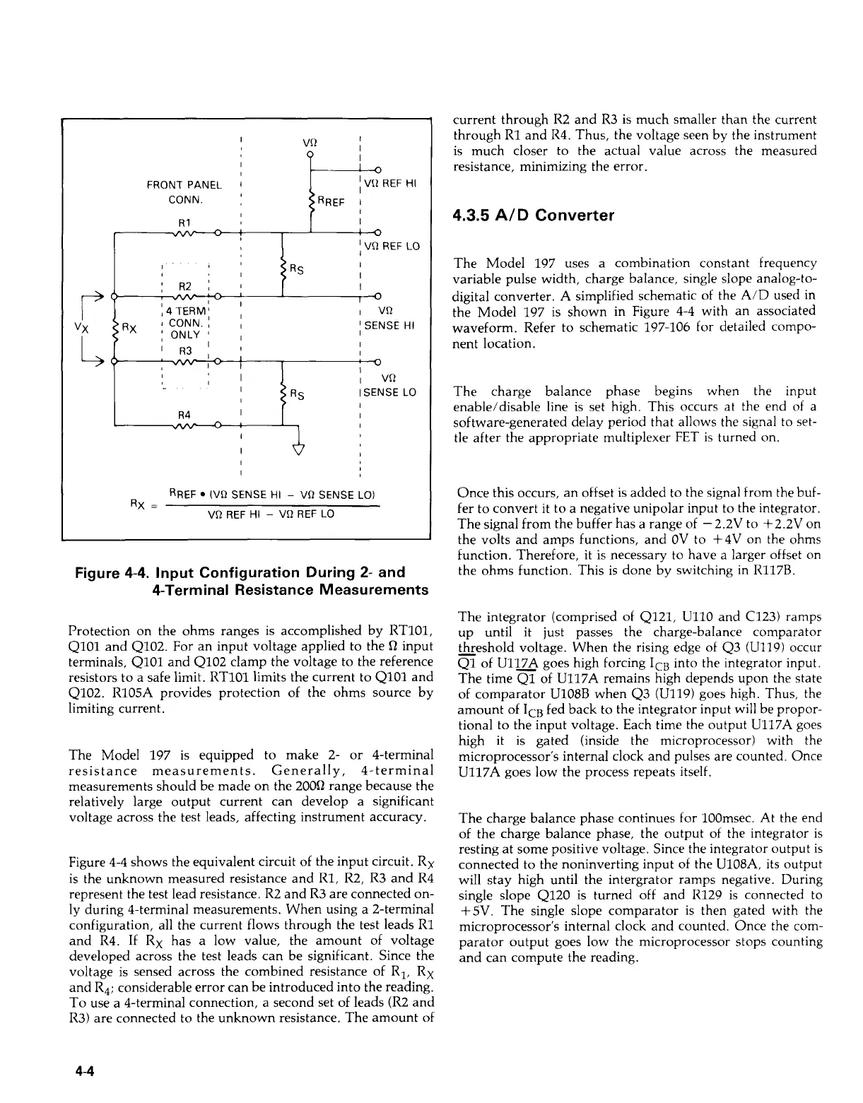
Figure 4-4. Input Configuration During
2-
and
4-Terminal Resistance Measurements
Protection on the ohms ranges is accomplished by RT101,
QlOl
and Q102. For an input voltage applied to the
3
input
terminals,
QlOl
and Q102 clamp the voltage to the reference
resistors to a safe limit. RT101 limits the current to
QlOl
and
Q102. R105A provides protection of the ohms source by
limiting current.
The Model 197 is equipped to make 2-
or
4-terminal
resistance measurements. Generally, 4-terminal
measurements should be made on the 2003 range because the
relatively large output current can develop a significant
voltage across the test leads, affecting instrument accuracy.
Figure 4-4 shows the equivalent circuit of the input circuit. Ry
is the unknown measured resistance and R1,
R2,
R3
and R4
represent the test lead resistance. R2 and
R3
are connected on-
ly during 4-terminal measurements. When using a 2-terminal
configuration, all the current flows through the test leads
R1
and R4.
If
Rx
has a low value, the amount of voltage
developed across the test leads can be significant. Since the
voltage is sensed across the combined resistance of
Rl,
Rx
and
R,;
considerable error can be introduced into the reading.
To use a 4-terminal connection, a second set of leads
(R2
and
R3) are connected to the unknown resistance. The amount of
current through
R2
and
R3
is much smaller than the current
through
R1
and R4. Thus, the voltage seen by the instrument
is much closer to the actual value across the measured
resistance, minimizing the error.
4.3.5
A/D
Converter
The Model 197 uses a combination constant frequency
variable pulse width, charge balance, single slope analog-to-
digital converter.
A
simplified schematic of the AID used in
the Model 197
is
shown in Figure 4-4 with an associated
waveform. Refer to schematic 197-106 for detailed compo-
nent location.
The charge balance phase begins when the input
enable/disable line is set high. This occurs at the end
of
a
software-generated delay period that allows the signal
to
set-
tle after the appropriate multiplexer
FET
is turned on.
Once this occurs, an offset is added to the signal from the buf-
fer to convert
it
to a negative unipolar input to the integrator.
The signal from the buffer has a range of -2.2V to +2.2V on
the volts and amps functions, and
OV
to +4V on the ohms
function. Therefore, it is necessary
to
have a larger offset
on
the ohms function. This is done by switching
in
R117B.
The integrator (comprised of 4121, UllO and
C123)
ramps
up until
it
just passes the charge-balance comparator
threshold voltage. When the rising edge of Q3 (U119) occur
of U11LA goes high forcing
IcB
into the integrator input.
The time
Q1
of U117A remains high depends upon the state
of comparator
U108B
when Q3 (U119) goes high. Thus, the
amount of
I,,
fed back to the integrator input will be propor-
tional to the input voltage. Each time the output U117A goes
high
it
is gated (inside the microprocessor) with the
microprocessor's internal clock and pulses are counted. Once
U117A goes low the process repeats itself.
The charge balance phase continues for 100msec. At the end
of the charge balance phase, the output of the integrator is
resting at some positive voltage. Since the integrator output is
connected to the noninverting input of the U108A, its output
will stay high until the intergrator ramps negative. During
single slope Q120 is turned off and R129 is connected to
+5V. The single slope comparator is then gated with the
microprocessor's internal clock and counted. Once the com-
parator output goes low the microprocessor stops counting
and can compute the reading.
4-4
Artisan Technology Group - Quality Instrumentation ... Guaranteed | (888) 88-SOURCE | www.artisantg.com