5-14 Keysight N5221A/22A Service Guide
Theory of Operation
Synthesized Source Group Operation
5-
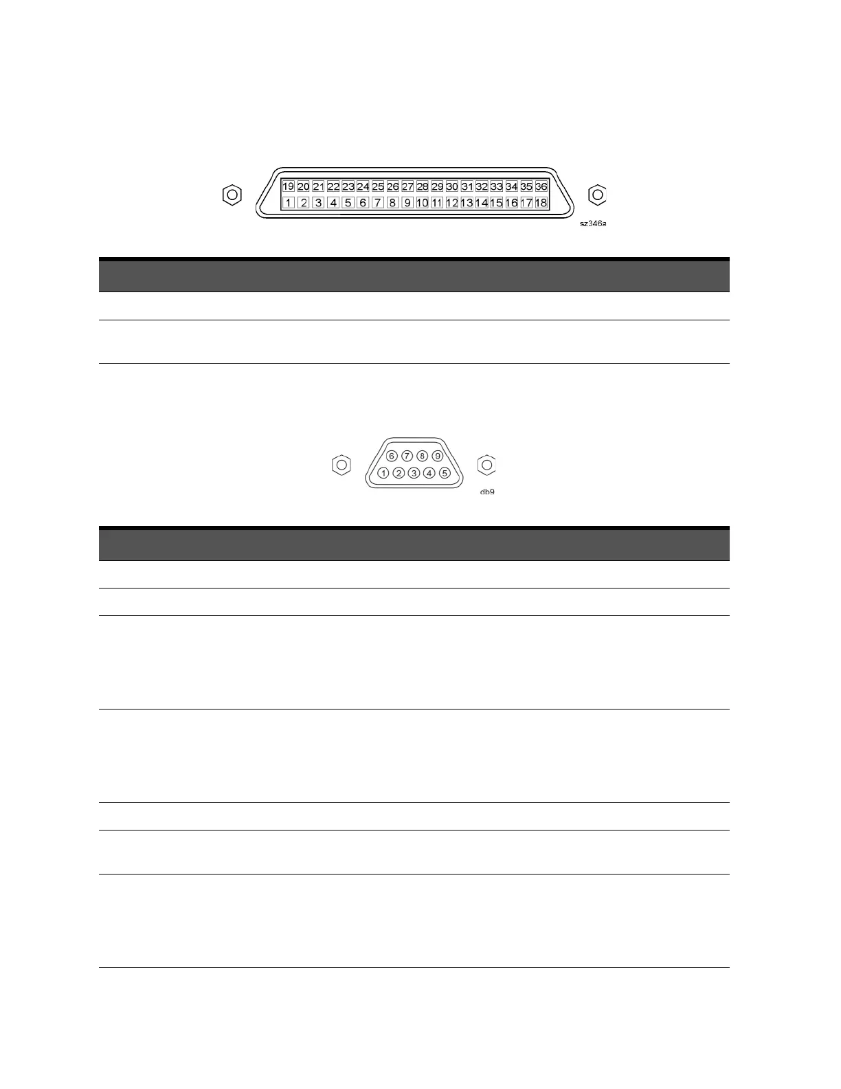
35 Sweep End TTL out, active low (10 μs min) indicates sweep done
36 Pass/Fail Write
Strobe
TTL out, active low pass/fail write strobe (1 μs min)
Table 5-3 PWR I/O Connector Pin Assignments
DB-9 Female Connector
Pin Name Description
1 +15V +15 V @ 400 mA
2 -15V -15 V @ 400 mA
3 AnalogOut1 Analog Output Voltage
Programmable ±10 V @ 100 mA out
Nominally 0 ohms
2.44 mV typical resolution
1 MHz BW
4 AnalogOut2 Analog Output Voltage
Programmable ±10 V @ 100 mA out
Nominally 0 ohms
2.44 mV typical resolution
1 MHz BW
5 ACOM System ground
6 GndSense Ground sense for Analog In and Analog Out
Connected with 51.1 ohms to ACOM
7 AnalogIn1 Analog input:
±10 V @ 1.22 mV typical resolution
Rin > 1 M-ohm
BW ≈ 1 MHz
ADC conversion time < 1 us typical
Table 5-2 HANDLER I/O Connector Pin Assignments
Rectangular 36-Pin Female Connector
Pin Numbers Name Function