Keysight N5221A/22A Service Guide 5-13
Theory of Operation
Synthesized Source Group Operation
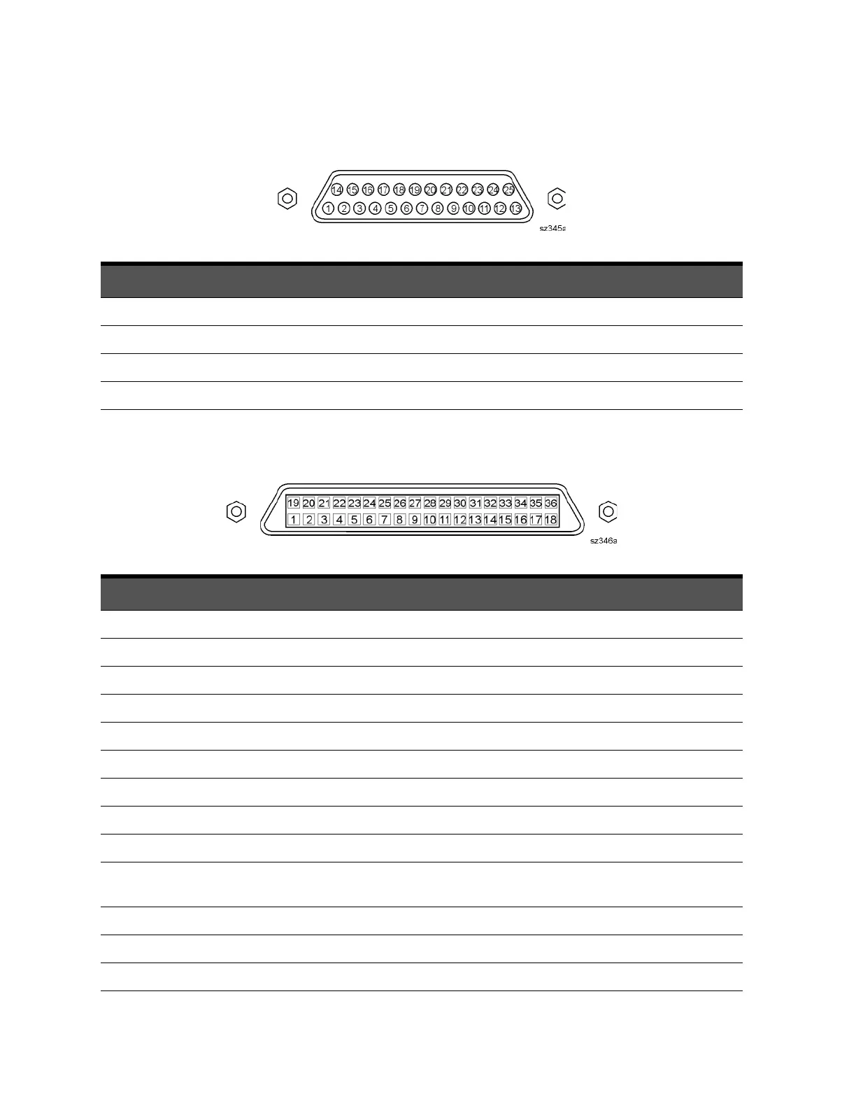
19–21 AD7–5 TTL I/O, address and latched data
22–23 AD0–1 TTL I/O, address and latched data
24 LDS TTL out, active low data strobe (1 μs min)
25 RLW TTL out, high = read, low = write
Table 5-2 HANDLER I/O Connector Pin Assignments
Rectangular 36-Pin Female Connector
Pin Numbers Name Function
1 GND 0 V, ground reference
2 INPUT1 TTL in, negative pulse (1 μs min) latches OUTPUT1-2
3–4 OUTPUT1–2 TTL out, latched
5–12 Port A0–7 Out TTL out, latched
13–20 Port B0–7 Out TTL out, latched
21–24 Port C I/O TTL I/O, latched
25–28 Port D I/O TTL I/O, latched
29 Port C Status TTL out, low = input mode, high = output mode
30 Port D Status TTL out, low = input mode, high = output mode
31 Output Strobe
Write Strobe
TTL out, active low data write strobe (1 μs min)
32 No connect Not used
33 Pass Fail TTL out, latched, indicates pass fail (programmable polarity)
34 +5 V +5 Vdc, 100 mA max.
Table 5-1 TEST SET I/O Connector Pin Assignments
DB-25 Female Connector
Pin Numbers Name Function