55
ECP5 and ECP5-5G High-Speed I/O Interface
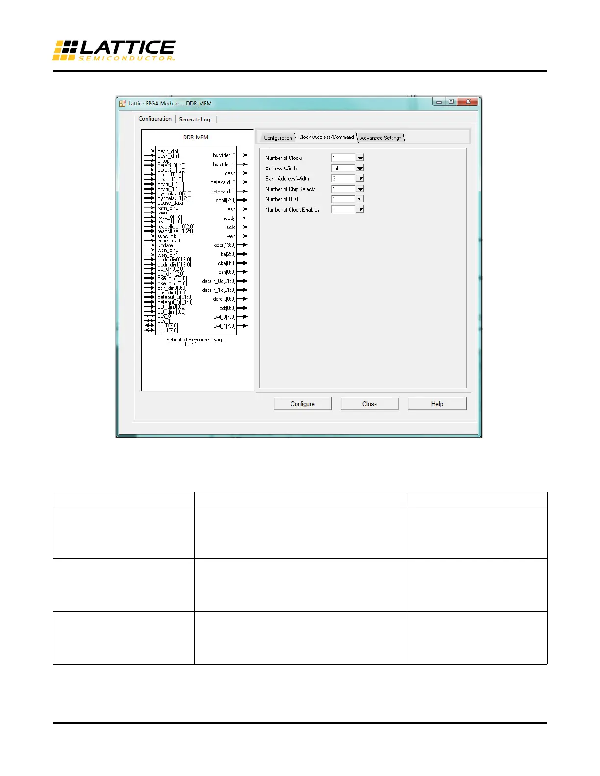
Figure 48. DDR_MEM Clock/Address/Command Tab
Table 12 lists the values that can be used for the Clock/Address/Command settings.
Table 12. DDR_MEM Clock/Address/Command Parameters
GUI Option Range Default Value
Number of Clocks DDR2: 1, 2, 4
DDR3: 1, 2, 4
DDR3L: 1, 2, 4
LPDDR2: 1
LPDDR3: 1
DDR3: 1
DDR2: 1
DDR3L: 1
LPDDR2: 1
LPDDR3: 1
Address Width DDR2: 13 – 16
DDR3: 13 – 16
DDR3L: 13 – 16
LPDDR2: Blank
LPDDR3: Blank
DDR2: 13
DDR3: 14
DDR3L: 14
LPDDR2: Blank
LPDDR3: Blank
Bank Address Width DDR2: 2, 3
DDR3: 3
DDR3L: 3
LPDDR2: Blank
LPDDR3: Blank
DDR2: 2
DDR3: 3
DDR3L: 3
LPDDR2: Blank
LPDDR3: Blank
 Loading...


