can support, or more than its negotiated limit, the Host will disconnect the downstream offending port (This
description does not include the new Battery Charging Spec BC 1.2 ECN to the USB 2.0 specification).
T
able 11-3. USB Modes and Data Rates Summary
USB Modes Clock Accuracy Data Rate
HS: High Speed ±0.05% 480Mb/s
FS: Full Speed ±0.25% 12 Mb/s
LS: Low Speed ±1.5% 1.5 Mb/s
Table 11-4. USB Transfer Types and Error Retry Summary
USB Data Transfer Types
Auto Resend on CRC
error
Use Cases
Control Transfer YES Used to configure the device (Enumeration)
Interrupt Transfer YES
Used to send short, simple data like keyboard, mouse, touch pad, touchscreen, or
game controller
.
Bulk Transfer YES
Used to transfer large amounts of data like files, pictures, printer data with 100%
accuracy.
Isochronous Transfer NO Used for streaming video and audio.
Note: CRC checks are done automatically by the USB hardware. At transmission, the packet CRC is encoded in the
packet header
. On packet reception the CRC of the data packet is calculated again and compared to the transmitted
encoded CRC value in the packet.
• The two most common design issues related to USB are signal integrity due to impedance mismatches and
timing violations. The following figure shows what is called a USB eye diagram. The area in RED represents a
restricted area that a USB signal cannot intersect, or it will not be in compliance with the USB specifications.
Such a violation can cause CRC errors and dropped packets.
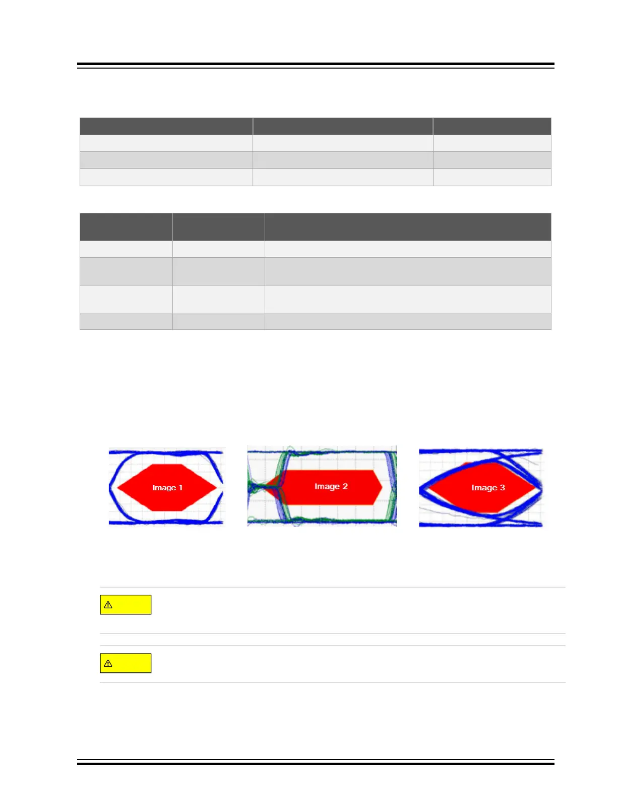
Figure 11-9. USB EYE Diagram
• Image 1 represents a passing USB differential eye diagram with excellent timing, rise or fall times and
impedance matching.
•
Image 2 represents a timing issue associated usually with USB source clock accuracy and jitter issues.
Ensure that the combined MCU clock source plus any used PLL and DFLL used to supply the USB
clock meet the clock accuracy requirements in the USB Modes and Data Rates Summary table listed
above.
If using a PLL or DFLL to supply the USB clock, check the data sheet jitter spec if listed, or calculate
using the formula provided in the data sheet to insure it meets the accuracy specifications again.
• Image 3 represents a typical impedance mismatch issue either due to PCB layout, component selection that is
in contact with the D+ and D- signal, or the use of a non-certified USB cable.
Serial Data Corruption Errors
© 2022 Microchip T
echnology Inc.
and its subsidiaries
Manual
DS70005439B-page 44