-
The SC3 signal at U102 pin 14 controls the Rx 5V switch U106, and
the receive 5 volts (R5). A voltage on the synthesizer SOUT line at
U204 pin 19 supplies power (Vcc) to the VCO buffer at U201 pin 3.
During the receive mode, regulator U106 supplies regulated 5V (R5) to
the receiver front end. In the battery-saver mode, R5 can be switched
on and off by controlling pin 3 of U106. Module U106 is not used
during the transmit mode. During the transmit mode, transmit 5 volts
(T5) for the ALC IC and other TX circuitry is obtained from U202 via
switching transistor Q111.
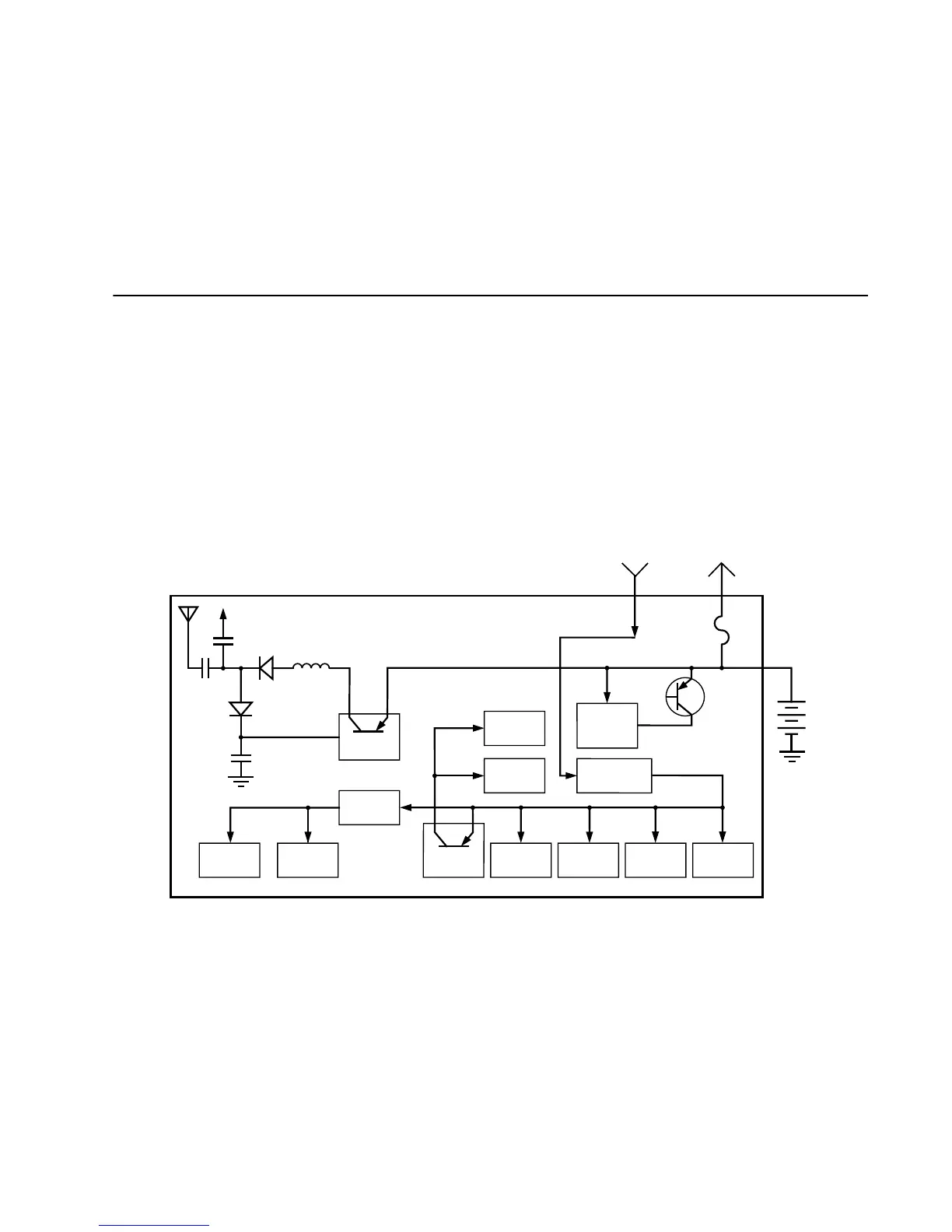
B+ Routing for
800MHz
Transceiver Boards
Refer to Figure 2 and your specific schematic diagram.
Raw B+ (7.5V) from the battery (Batt B+) enters the radio on the
transceiver board through a 3-contact spring pin arrangement (J3) as
B+, where it is routed through four ferrite beads (E1, E2, E3, E4) and
applied to the RF power amplifier (U502) and the ALC IC (U504 pin
13). Battery B+ is fused and then routed to the VOCON board, where
it enters on connector J1 pins 19 and 20. On secure radios, Raw B+ is
also routed to the encryption board so that it can perform key
management and other functions independently of SW B+.
The SW B+ is applied to the 5V regulator (U505) to produce a stable
5.0 volt output. Regulator U505 supplies those circuits which need to
remain on at all times, such as the reference oscillator (U304),
fractional-n-synthesizer (U302), D/A IC (U503), and the ABACUS IC
(U401). The D/A IC controls dc switching of the transceiver board. The
SCI signal at U503 pin 12 controls Q503 and transmit 5 volts (T5). The
SC3 signal at U503 pin 14 controls the RX 5V switch in Q503 and the
Figure 2 . B+ Routing for 800MHz Transceiver Boards
Ref Osc
U304
ABACUS
U401
D/A IC
U503
Synth
U302
VCOB IC
U303
VCO
U307
5V Regulator
U505
RF PA
Module
U502
RF Amp
U202
Mixer
U205
Q503
ALC
U504
Rx
800MHz Transceiver Board
5V
SW B+ Raw B+
UNSW B+
IF Amp
Q601
MAEPF-24336-O
CR104
L101
CR102
Fuse
Battery
7.5V
+
To/From VOCON Board
 Loading...