10-9
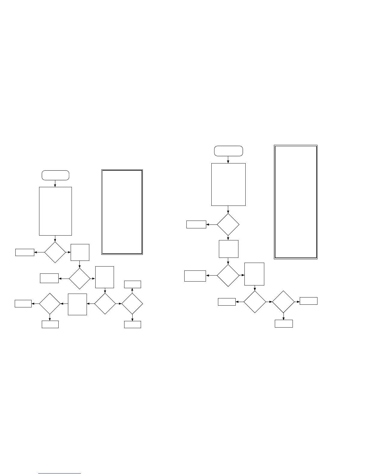
Chart 13 . 02/88, DSP External SRAM Failure U414
R3SEL*
appears
functional?
Yes
Replace U414.
Do all three
SRAMs
exhibit a
fault?
Replace U405.
Yes
MAEPF-24410-A
No
No
ADSIC
checksum
error?
Refer to
section on
FAIL 02/A0.
Chart C.11
Yes
No
During power
up Self-Test
verify E1~ on
U414 is enabled
by high to low
transitions of
R3SEL*.
During power-up
verify operation
of U415 by
looking for
transitions on
inputs IN_B and
IN_A.
Inputs to
U415
functional?
Replace U415.
Replace U405.
Yes
No
Synopsis
On power-up the DSP writes
data to the device and then
verifies the data. This failure
indicates the DSP SRAM failed
this pattern/checksum test.
U414 is selected by the DSP
(U405) address bus with the
addition of the OR logic gate
U415. Basic failure modes
are as follows:
1) Some problem exists
(open/shorts) with the
external address/data bus.
2) Possible failure of the DSP
address/data bus or
RD*/WR*/PS*/DS* signals
used in selecting this part.
Since the other two DSP
SRAMs share this bus as well
as other ICs, this is not a likely
failure.
3) Operational failure of the OR
logic of gate U415.
3) Open in supply or ground to
the IC.
4) Failure of the IC.
Fail 02/88
DSP SRAM U414
Failure
Use ohmmeter to
electrically verify
following signal connections
to source IC:
Signal @ U414 Source
D0-D23 U405
A0-A12 U405
WR*,RD* U405
E1* U415-OUT
E2 U406-A15
X/Y*,V/S* GND
VCC +5V
VSS GND
Signal @ U415 Source
IN_A U405-A14
IN_B U405-A13
Connections
good?
Repair opens.
Yes
No
Check for
ADSIC
programming
checksum
error.
Chart 14 . 02/84, DSP External SRAM Failure U403
Fail 02/84
DSP SRAM U403
Failure
Synopsis
On power-up the DSP writes
data to the device and then
verifies the data. This failure
indicates the DSP SRAM failed
this pattern/checksum test.
Besides utiling decoding logic
from the DSP (U405), U403
has additional logic in the form
of RSEL from the ADSIC
(U406). A problem with the
ADSIC in the form of a
programming or hardware fault
will cause a problem with the
operation of this part. Basic
failure modes are as follows:
1) Some problem exists
(open/shorts) with the
external address/data bus.
2) Some problem exists with
the ADSIC memory select
(RSEL) which may include an
ADSIC programming problem
(SPI bus) or possibly a failed
ADSIC.
3) Possible failure of the DSP
address/data bus or
RD*/WR*/PS*/DS* signals
used in selecting this part.
Since the other two DSP
SRAMs share this bus as well
as other ICs, this is not a likely
failure.
4) Open in supply or ground to
the IC.
5) Failure of the IC.
Use ohmmeter to
electrically verify
following signal connections
to source IC:
Signal @ U403 Source
D0-D23 U405
A0-A12 U405
WR*,RD* U405
E1* U405-A15
E2 U406-RSEL
X/Y*,V/S* GND
VCC +5V
VSS GND
RSEL
appears
functional?
Yes
Replace
U406.
Replace U403.
Do all three
SRAMs
exhibit a
fault?
Replace U405.
MAEPF-24409-B
Yes
No
No
Connections
good?
Repair opens.
Yes
No
Check for
ADSIC
programming
checksum
error.
ADSIC
checksum
error?
Refer to
section on
FAIL 02/A0.
Chart C.11
Yes
No
During power
up Self-Test
verify E2 on
U403 is enabled
by low to high
transitions of
RSEL.
 Loading...