MC68705U3 AND MC68705U5
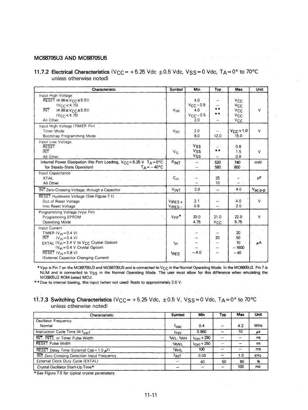
11.7.2 Electrical Characteristics
(Vee=
+5.25
Vdc ±O.5 Vdc,
VSS=O
Vdc,
TA=Oo
to
70
0
e
unless
otherwise noted)
Characteristic
Symbol Min Typ Max Unit
Input High Voltage
RESET
(4.99SVCCs5.51) 4.0
-
VCC
(VCC<4.75)
VCC-0.5
-
VCC
INT (4.99SVCCs5.51)
VIH
4.0
**
VCC
V
(VCC<4.75)
VCC-0.5
**
VCC
All Other
2.0
-
VCC
Input High Voltage (TIMER
Pin)
Timer Mode
VIH
2.0
-
VCC+l.0
V
Bootstrap Programming Mode 9.0 12.0 15.0
Input
Low Voltage
RESET
VSS
-
0.8
INT
VIL
VSS
**
1.5 V
All Other
VSS
-
0.8
Internal
Power Dissipation (No Port Loading,
VCC=
5.25 V T A =O°C·
PINT
-
520
740
mW
for
Steady-State Operation)
TA=
-40°C
-
580
800
Input Capacitance
XTAL
Cin
-
25
-
pF
All Other
-
10
-
INT Zero-Crossing Voltage. through a Capacitor
VINT
2.0
-
4.0
Vac p-p
RESET
Hysteresis Voltage (See Figure 7-1)
Out of
Reset
Voltage
VIRES
+
2.1
- 4.0
V
Into
Reset
Voltage
VIRES-
0.8
- 2.0
Programming Voltage. (Vpp
Pin)
Programming
EPROM
Vpp*
20.0 21.0 22.0 V
Operating Mode
4.75
VCC
5.75
Input Current
TIMER (Vin = 0.4
V)
-
-
20
INT
(Vin=O.4
V)
-
20
50
EXTAl
(Vin=2.4
V to
VCC
Crystal Option)
lin
-
-
10
p.A
(Vin = 0.4 V Crystal Option) -
-
-1600
RESET
(Vin=0.8
V)
IRES
-4.0
-
-40
(External Capacitor Changing Current)
*Vpp
is
Pin
7
on
the MC68705U3 and MC68705U5 and
is
connected
to
VCC
in
the Normal Operating Mode. In the MC6805U2.
Pin
7
is
NUM and
is
connected to VSS in the Normal Operating Mode. The user must allow
for
this difference when emulating the
MC6805U2 ROM-based
MCU.
* * Due to internal biasing. this input (when
not
used) floats
to
approximately 2.0
V.
11.7.3 Switching Characteristics
(Vee=
+5.25
Vdc, ±O.5
V,
VSS=O
Vdc,
TA=Oo
to
70
0
e
unless
otherwise noted)
Characteristic
Symbol
Min
Typ
Max
Unit
Oscillator Frequency
Normal
fosc
0.4 -
4.2
MHz
Instruction Cycle Time (4/fos
c
)
tcyc
0.950
-
10
"s
iNT.
INT2. or Timer
Pulse
Width
tWL.tWH
tcyc+
250
- -
ns
RESET
Pulse
Width
tRWL
tcyc+
250
-
-
ns
RESET
Delay Time (External Cap= 1.0
p.F)
tRHL
100
-
-
ms
INT Zero Crossing Detection Input Frequency
flNT
0.03
-
1.0
kHz
External
Clock Duty Cycle
(EXT
AU
-
40
50
60 %
Crystal Oscillator Start-Up
Time*
-
-
-
100
ms
*
See
Figure 7-5 for
tYPical
crystal parameters.
11-11
 Loading...

