MC68705U3
AND
MC68705U5
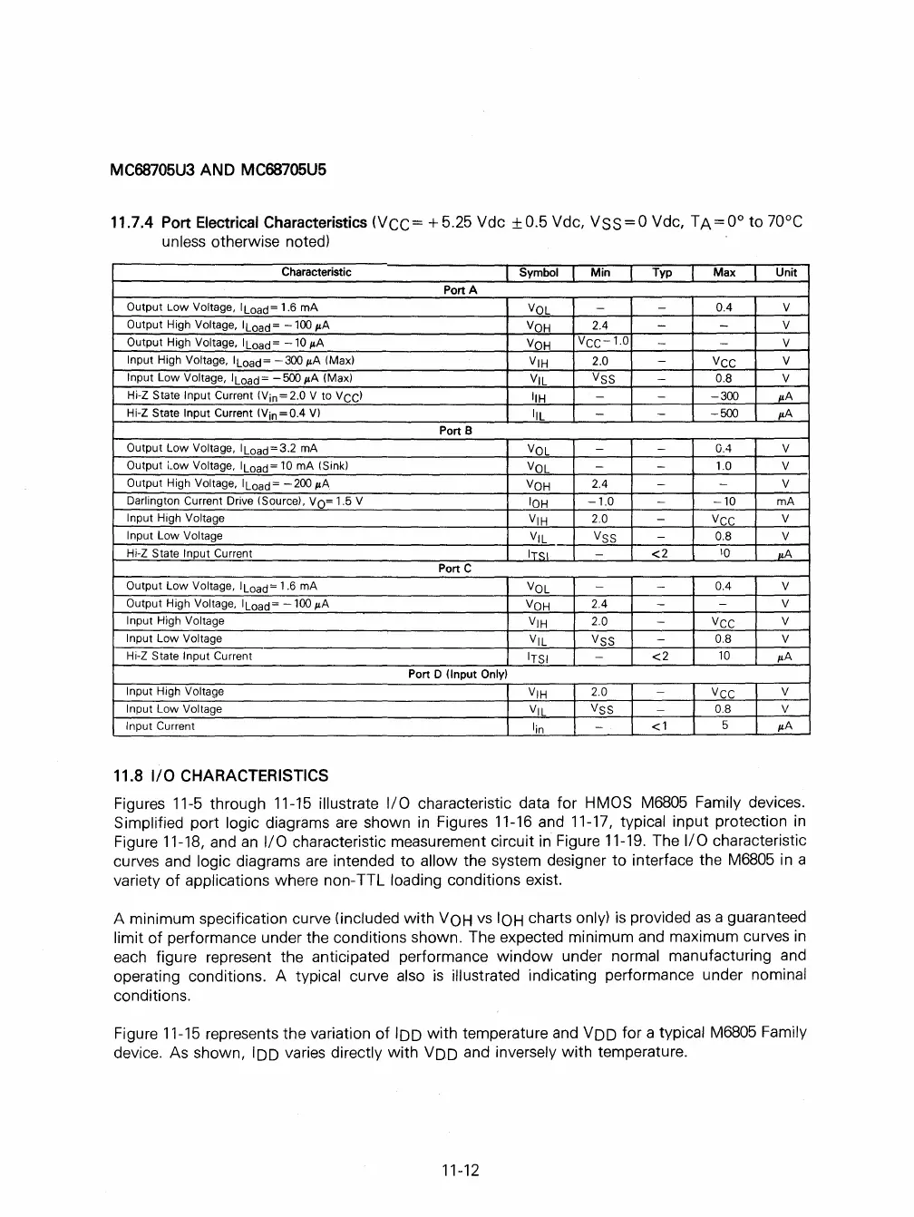
11.7.4 Port Electrical Characteristics
(Vee=
+5.25
Vdc ±O.5 Vdc,
VSS=O
Vdc,
TA=Oo
to
70
0
e
unless otherwise noted)
Characteristic
Symbol
Min
Typ Max Unit
Port A
Output Low Voltage,
ILoad= 1.6 mA
VOL
-
-
0.4
V
Output High Voltage, ILoad =
-100
/LA
VOH
2.4 - -
V
Output High Voltage,
ILoad=
-10
/LA
VOH
VCC-l.0
-
-
V
Input High Voltage, ILoad=
-300
/LA
(Max)
VIH
2.0
-
VCC
V
Input Low Voltage, ILoad=
-500
/LA
(Max)
VIL
VSS
- 0.8 V
Hi-Z State
Input Current
(Vin=2.0
V to
VCC)
IIH
- -
-300
/LA
Hi-Z State Input Current (Vin = 0.4
V)
IlL
-
-
-500
/LA
Port B
Output Low Voltage,
ILoad=3.2
mA
VOL
- -
0.4 V
Output i.ow Voltage,
ILoad=
10
mA (Sink)
VOL
- -
1.0 V
Output High Voltage, ILoad=
-200
/LA
VOH
2.4
-
-
V
Darlington
Current Drive (Source), VO= 1.5 V
10H
-1.0
-
-10
mA
Input High Voltage
VIH
2.0
-
VCC
V
Input Low Voltage
VIL
VSS
-
0.8 V
Hi·Z State Input Current
ITS
I
-
<2
10
p.A
Port C
Output Low Voltage, ILoad= 1.6 mA
VOL
-
- 0.4 V
Output High Voltage,
ILoad=
-100
/LA
VOH
2.4
-
-
V
Input High Voltage
VIH
2.0
-
VCC
V
Input Low Voltage
VIL
VSS
- 0.8
V
Hi·Z State Input Current
ITSI
-
<2
10
/LA
Port 0 (Input Only)
Input High Voltage
VIH
2.0
-
VCC
V
Input Low Voltage
VIL
VSS
-
0.8 V
Input Current
lin
-
<1
5
/LA
11.8
I/O
CHARACTERISTICS
Figures 11-5 through 11-15 illustrate
I/O
characteristic data for HMOS M6805 Family devices.
Simplified port logic diagrams are shown
in
Figures 11-16 and 11-17, typical input protection
in
Figure 11-18, and
an
I/O
characteristic measurement circuit in Figure 11-19. The
I/O
characteristic
curves and logic diagrams
are
intended
to
allow the system designer
to
interface the M6805 in a
variety
of
applications where non-TTL loading conditions exist.
A minimum specification curve (included
with
VOH vs
10H
charts only)
is
provided
as
a guaranteed
limit
of
performance under the conditions shown. The expected minimum and maximum curves
in
each figure represent the anticipated performance
window
under normal manufacturing and
operating conditions. A typical curve also
is
illustrated indicating performance under nominal
conditions.
Figure 11-15 represents the variation
of
100
with
temperature and
VOO
for a typical M6805 Family
device. As shown,
100 varies directly
with
Von
and inversely
with
temperature.
11-12
 Loading...

