Issue 2 06/2005 COMPANY CONFIDENTIAL 27
Copyright © 2005 Nokia. All Rights Reserved.
RH-53/54
Nokia Customer Care
Troubleshooting
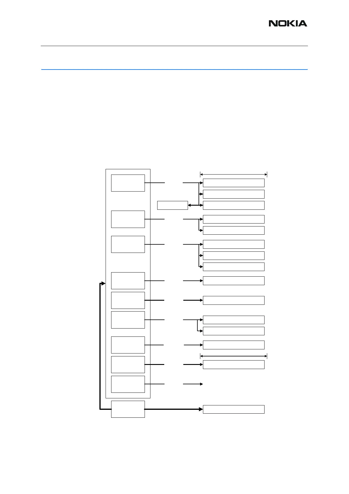
■ Common circuit
The power supply and the synthesiser is common for RH53/54, except for the synthesiser rang-
es.
Power Supply Configuration
All power supplies for the RF Unit are generated in the UEM IC (D200). All power outputs from
this IC have a decoupling capacitor at which the supply voltage can be checked.
The power supply configuration used in the phone is shown in the block diagram below:
Figure 18:Power supply configuration
UEM
Internal Mjoelner
VCO module
Front End Module
Vbat
VCO
VR7
2.78 V +/- 3%
@45 mA
VIO
Digital com. interface
1.8 V +/- 4.5%
@150 mA
VR6
LNA and Pre-gain
BB Section
2.78 V +/-3%
@50 mA
VrefRF01
Ref. volt for Mjoelner
1.35 V +/- 2%
< 100 uA
PLL charge pump
VR1a
4.75 V +/-3%
@10 mA
PLL Counters
PLL Pre-scaler
Dividers & LO buffer
VR5
2.78 V +/-3%
@50 mA
Baseband clk buffer
VCXO Power Supply
VR3
2.78 V +/-3%
@20 mA
VR2
TX modulator
2.78 v +/-3%
@100 mA
Power Loop Amp
Digital control logic
Modulator loading
netwok
VR4
2.78 V+/- 3%
@50 mA
Not used
 Loading...