Signal
name/
RAP3G
Signal
name/ SD
Card
Signal Properties
Direction -- Levels -- Freq./Timing
Resolution
Descriptio
n / Notes
GenIO 06 SD Write
Protect
< 0-1.8 V /
0-3.6V
Write
protect
detection
, used
only with
normal
size SD
Card
GenIO 02 MMCFBClk < 0-1.8 V /
0-3.6V
Clock
Feedback
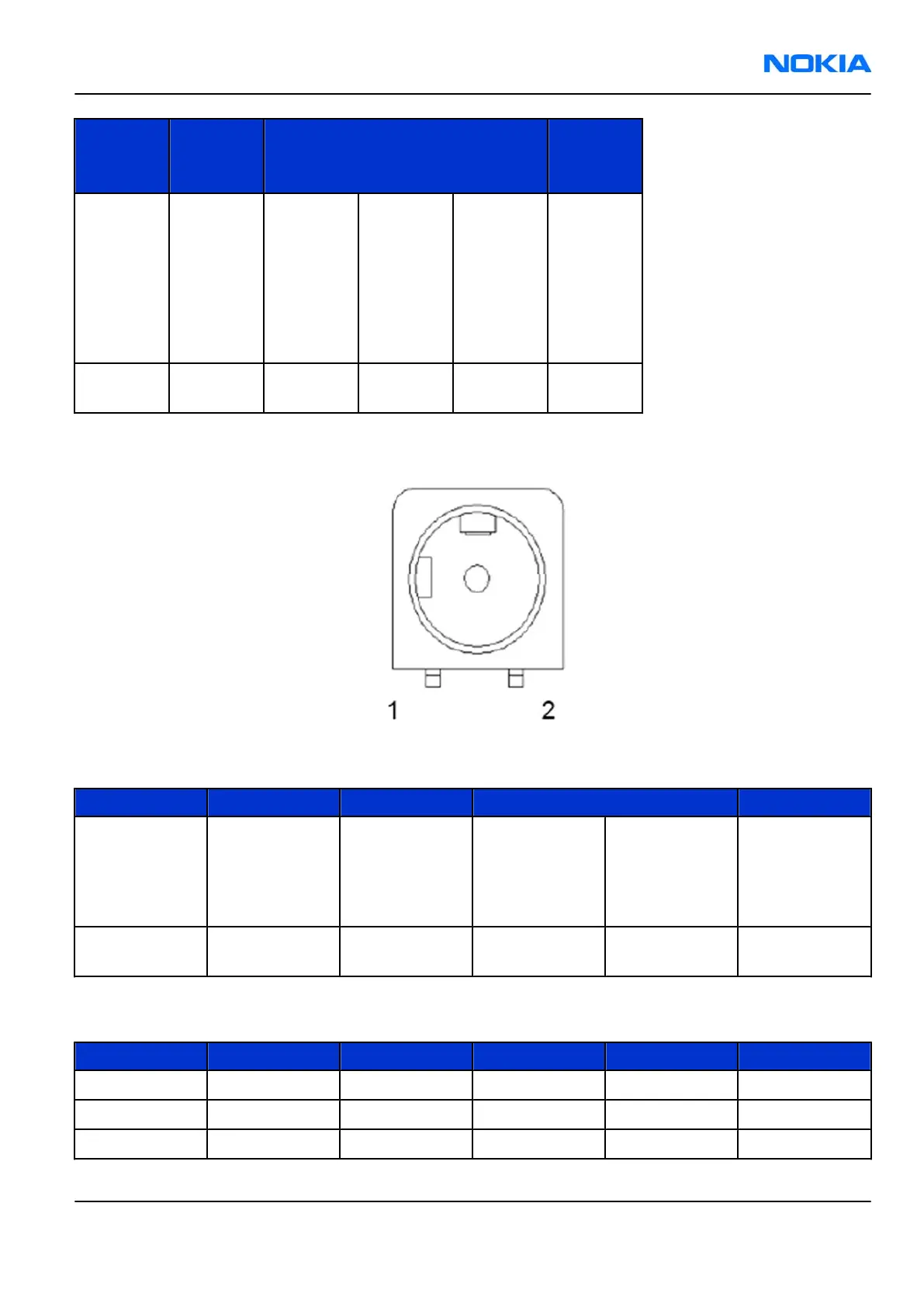
Charger connector and charging interface connections & electrical characteristics
Figure 64 Charger connector
Table 16 Charging interface connections
Pin Signal I/O Engine connection Notes
1 Vchar In N2300 VCharIn1, 2 Charging
voltage /
charger
detection,
Center pin
2 Charge GND Ground Charger
ground
Table 17 Charging IF electrical characteristics
Description Parameter Min Max Unit Notes
Vchar V Charge 0 9 V Center pin
Vchar I Charge 0.85 A Center pin
Charge GND 0.85 A
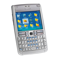
RM-88
System Module Nokia Customer Care
Issue 1 COMPANY CONFIDENTIAL Page 8 –23
Copyright © 2006 Nokia. All rights reserved.